Question: $ 0 4 - 2 0 2 4 - 1 0 0 4 - 7 0 4 CSCI 1 5 0 3 . ( 5
$
CSCI
pt Combinational Circuit designs
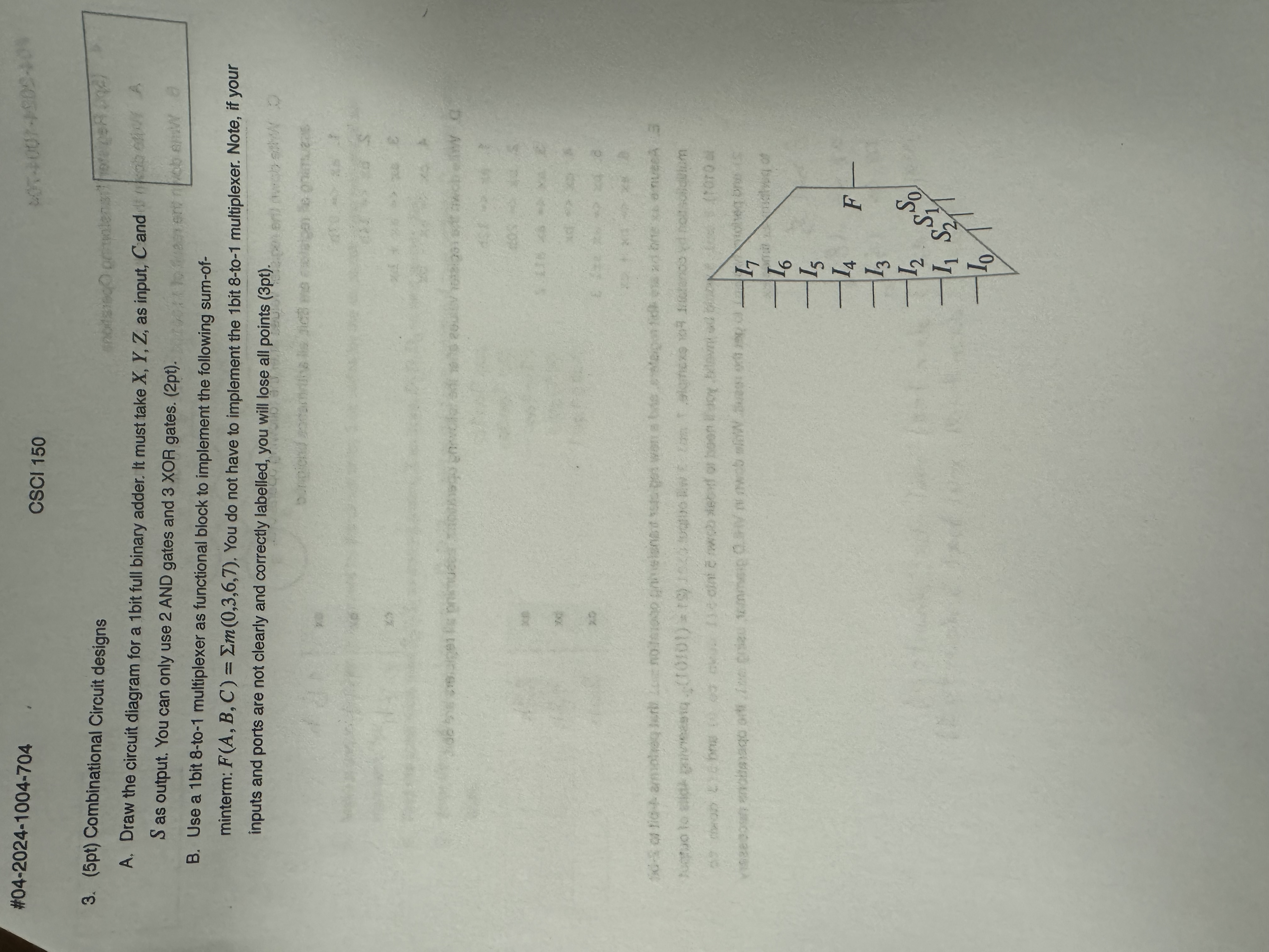
A Draw the circuit diagram for a bit full binary adder. It must take as input, and as output. You can only use AND gates and XOR gates. pt
B Use a bit to multiplexer as functional block to implement the following sumofminterm: You do not have to implement the bit to multiplexer. Note, if your inputs and ports are not clearly and correctly labelled, you will lose all points pt

Step by Step Solution
There are 3 Steps involved in it
1 Expert Approved Answer
Step: 1 Unlock


Question Has Been Solved by an Expert!
Get step-by-step solutions from verified subject matter experts
Step: 2 Unlock
Step: 3 Unlock


