

Question: 0 . 4 ( 2 0 p t s ) Consider the p - n junction below with a negligibly small depletion layer width. Intrinsic
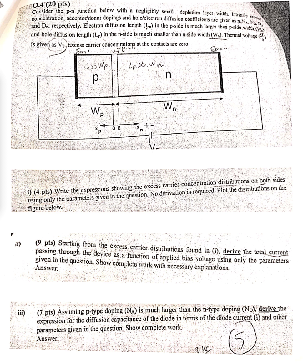
Consider the pn junction below with a negligibly small depletion layer width. Intrinsic cartie concentration, acceptordonor dopings and hole'electron diffusion coefficients are given as and respectively. Electron diffusion length in the p side is much larger than p side widh and hole diffusion length in the side is much smaller than side width Thermal voltage is given as Excess carrier concentrations at the contacts are zero.
i pts Write the expressions showing the excess carrier concentration distributions on both sides using only the parameters given in the question. No derivation is required. Plot the distributions on the figure below.
ii pts Starting from the excess carrier distributions found in i derive the total current passing through the device as a function of applied bias voltage using only the parameters given in the question, Show complete work with necessary explanations. Answer:
iii pts Assuming ptype doping is much larger than the ntype doping derive the expression for the diffusion capacitance of the diode in terms of the diode current I and other parameters given in the question. Show complete work. Answer:
Step by Step Solution
There are 3 Steps involved in it
1 Expert Approved Answer
Step: 1 Unlock

Question Has Been Solved by an Expert!
Get step-by-step solutions from verified subject matter experts
Step: 2 Unlock
Step: 3 Unlock