

Question: 1. Consider the first circuit shown below. Note that Pin #6 for mode selection is grounded to permanently put the IC in the shift mode.
1. Consider the first circuit shown below. Note that Pin #6 for mode selection is grounded to permanently put the IC in the shift mode.
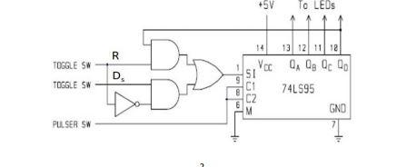
Thus, the circuit can operate as a SIPO/SISO shifter or a ring counter depending on R input provided by a toggle switch. That is, the serial data (DS) should be connected to the SI input of 74LS95 in case the circuit operates as a SIPO/SISO shifter. On the other hand, QD should be connected to the SI input in case of a ring counter. In the circuit, the SOP (Sum-ofProducts) logic circuit is used to provide a proper data to the SI input. Note an SOP-type logic is a circuit consists of an OR gate, each input of which is connected to the output of an AND gate. Derive the Boolean expression for SI as a function of R, QD, and DS. SI = ____________________________________________________________
2. Identify the logic level of R when the circuit operates as a ring counter: R = ________
3. Finally, derive a circuit equivalent to the SOP logic circuit using only one quad NAND gate IC.
SI = ______________________________________________________________
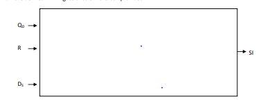
4. Draw the derived NAND gate circuit in the box provided.
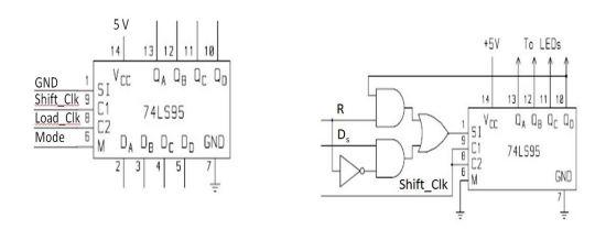
5. Now, lets emulate a serial communication system by using two 74LS95 shift register ICs: one operating in the PISO mode to emulate a transmitter and the other in the SIPO mode to emulate a receiver. In case of PISO, the toggle switch for the Mode should be flipped to logic 1 for the parallel load mode. Well use 4 toggle switches to supply a 4-bit parallel data. The Load_Clk is provided by a pulser. Once the loading is accomplished, the Mode switch should be flipped to logic 0 to select the shift mode. The stored data will be transmitted, one bit per clock period through QD output port. Well use another pulser to supply the Shift_Clk. In case of SIPO, the toggle switch for the R input should be flipped to logic 0 to receive the serial data (QD) from the transmitter (PISO) connected to the DS input. Draw a circuit diagram showing all the necessary wire connections: you need two wires. Indicate the logic state of R in the diagram.
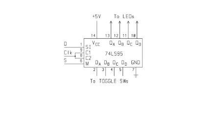
6. Design a Johnson counter by using a 74LS95 and one NAND gate. Show the circuit diagram below. Indicate the logic state of S for shift operation in the diagram.
+5V TO LEDs 14 R TOGGLE SW D. TOGGLE SW one 13 12 11 12 Voc In Og Qc Do SI C1 74L595 GND SD PULSER SW R + SI DS + 5V 14 +5V To LEDS 1 14 R GND Vec DA O QC Oo 51 Shift_Cik 9 C1 Load_Clke 74LS95 CZ Mode MDA DE OC DGND 23 Dy Va 0. Og Qc00 D. 74L595 4 5 GNO Shift_Clk 41 +5V TO LEOS - CIK 14 13 12 11 ta Voc DA Og OC D 51 9 B 74595 CZ 5 MDA DE Dc Dp GND 231 5 5 To TOGGLE SWS +5V TO LEDs 14 R TOGGLE SW D. TOGGLE SW one 13 12 11 12 Voc In Og Qc Do SI C1 74L595 GND SD PULSER SW R + SI DS + 5V 14 +5V To LEDS 1 14 R GND Vec DA O QC Oo 51 Shift_Cik 9 C1 Load_Clke 74LS95 CZ Mode MDA DE OC DGND 23 Dy Va 0. Og Qc00 D. 74L595 4 5 GNO Shift_Clk 41 +5V TO LEOS - CIK 14 13 12 11 ta Voc DA Og OC D 51 9 B 74595 CZ 5 MDA DE Dc Dp GND 231 5 5 To TOGGLE SWS
Step by Step Solution
There are 3 Steps involved in it

Get step-by-step solutions from verified subject matter experts