

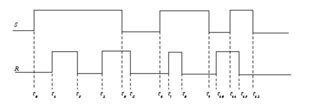
1. Draw the output(Q) timing diagram for a) NAND SR Latch and b) NOR SR Latch(Assume Q=1)....
Fantastic news! We've Found the answer you've been seeking!
Question:
1. Draw the output(Q) timing diagram for a) NAND SR Latch and b) NOR SR Latch(Assume Q=1). Assume gates have no delays
2. Derive a clocked SR Latch using NOR gates. Derive a D latch from this latch.
3. Draw 2 NOT gate feedback loop and 3 NOT gate feedback loop and find the difference in both their functionality.
Expert Answer:

Related Book For 

Business Law and the Legal Environment
ISBN: 978-1285860381
7th edition
Authors: Susan S. Samuelson, Jeffrey F. Beatty
Posted Date:
