

Question: 1. Write Verilog code for the logic circuit given in Figure 4.6. Simulate the circuit using Active-HDL and submit the Verilog code, input and
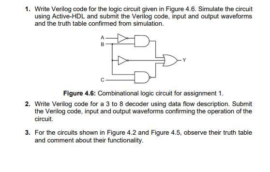
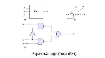
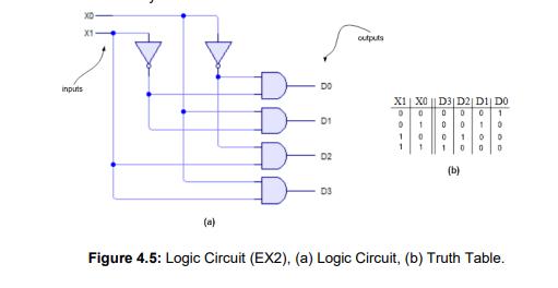
1. Write Verilog code for the logic circuit given in Figure 4.6. Simulate the circuit using Active-HDL and submit the Verilog code, input and output waveforms and the truth table confirmed from simulation. A B Figure 4.6: Combinational logic circuit for assignment 1. 2. Write Verilog code for a 3 to 8 decoder using data flow description. Submit the Verilog code, input and output waveforms confirming the operation of the circuit. 3. For the circuits shown in Figure 4.2 and Figure 4.5, observe their truth table and comment about their functionality. B (a) A (b) EX1 YI Jafe.. (c) Figure 4.2: Logic Circuit (EX1). inpurts XD- X1 (a) 8 DO D1 9 02 D3 outputs D 1 1 AOOOT X1 X0 || D3|D2| D1| DO D 0 0 0 D 0 1 0 1 0 0 1 1 0 1 0 n 8-000 (b) Figure 4.5: Logic Circuit (EX2), (a) Logic Circuit, (b) Truth Table.
Step by Step Solution
3.43 Rating (143 Votes )
There are 3 Steps involved in it
A inputs A B C B 0 0 O 0 0 1 O 01 1 ... View full answer

Get step-by-step solutions from verified subject matter experts