

Question: 12. In register transfer language, the READ operation from memory can be stated as: (a) R3 R1 + R2 (b) M[AR] R1 (c) R1 R2
![be stated as: (a) R3 R1 + R2 (b) M[AR] R1 (c)](https://dsd5zvtm8ll6.cloudfront.net/si.experts.images/questions/2024/09/66f3a8e84fa35_51966f3a8e7b0241.jpg)
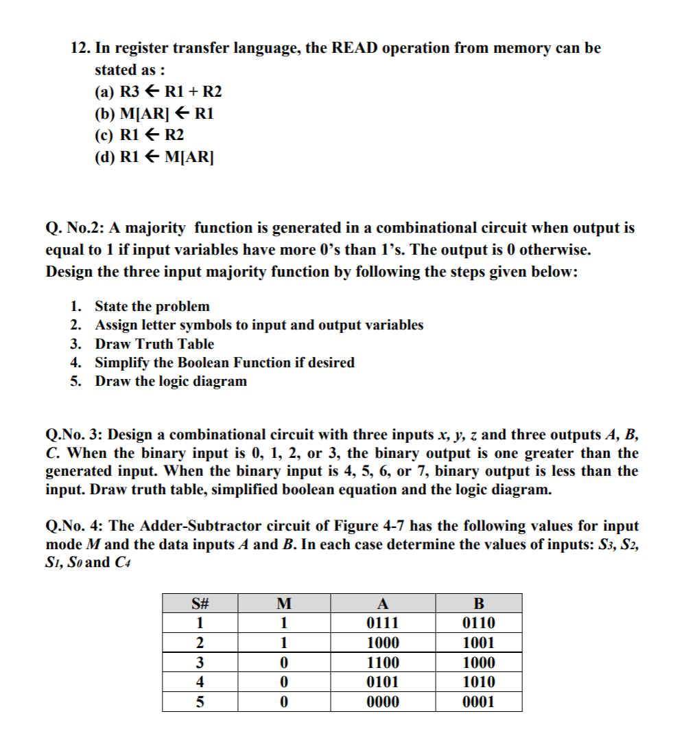
12. In register transfer language, the READ operation from memory can be stated as: (a) R3 R1 + R2 (b) M[AR] R1 (c) R1 R2 (d) R1 M[AR] Q. No.2: A majority function is generated in a combinational circuit when output is equal to 1 if input variables have more Os than ls. The output is 0 otherwise. Design the three input majority function by following the steps given below: 1. State the problem 2. Assign letter symbols to input and output variables 3. Draw Truth Table 4. Simplify the Boolean Function if desired 5. Draw the logic diagram Q.No. 3: Design a combinational circuit with three inputs x, y, z and three outputs A, B, C. When the binary input is 0, 1, 2, or 3, the binary output is one greater than the generated input. When the binary input is 4, 5, 6, or 7, binary output is less than the input. Draw truth table, simplified boolean equation and the logic diagram. Q.No. 4: The Adder-Subtractor circuit of Figure 4-7 has the following values for input mode M and the data inputs A and B. In each case determine the values of inputs: S3, S2, Si, So and C4 S# 1 2 3 4 5 M 1 1 0 0 A 0111 1000 1100 0101 0000 B 0110 1001 1000 1010 0001 0 Az A FA FA FA FA . S2 Figure 4-7 4-bit adder-subtractor, Q.No. 5: Design an arithmetic circuit with one selection variable S and two n-bit data inputs A and B. The circuit generates the following four arithmetic operations in conjunction with the input carry Cin. Draw logic diagram for first two stages. s Cin = 0 Cin = 1 0 D = A + B D = A +1 1 D= A-1 D = A-B *****************
Step by Step Solution
There are 3 Steps involved in it

Get step-by-step solutions from verified subject matter experts