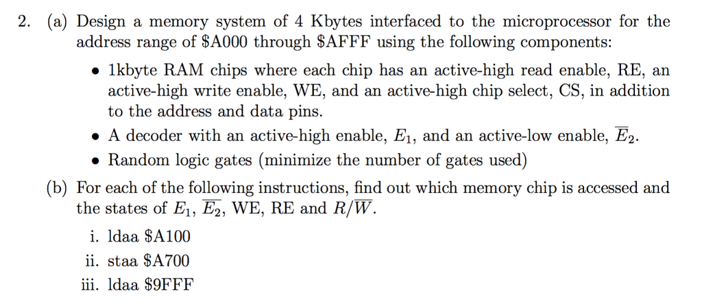
Question: 2. (a) Design a memory system of 4 Kbytes interfaced to the microprocessor for the address range of SA000 through SAFFF using the following components:

2. (a) Design a memory system of 4 Kbytes interfaced to the microprocessor for the address range of SA000 through SAFFF using the following components: |kbyte RAM chips where each chip has an active-high read enable, RE, an active-high write enable, WE, and an active-high chip select, CS, in addition to the address and data pins. A decoder with an active-high enable, E,, and an active-low enable. E2. Random logic gates (minimize the number of gates used) (b) For each of the following instructions, find out which memory chip is accessed and the states of E1, E2, WE, RE and R/W i. ldaa SA100 ii. staa SA700 iii. ldaa $9FFF 2. (a) Design a memory system of 4 Kbytes interfaced to the microprocessor for the address range of SA000 through SAFFF using the following components: |kbyte RAM chips where each chip has an active-high read enable, RE, an active-high write enable, WE, and an active-high chip select, CS, in addition to the address and data pins. A decoder with an active-high enable, E,, and an active-low enable. E2. Random logic gates (minimize the number of gates used) (b) For each of the following instructions, find out which memory chip is accessed and the states of E1, E2, WE, RE and R/W i. ldaa SA100 ii. staa SA700 iii. ldaa $9FFF
Step by Step Solution
There are 3 Steps involved in it

Get step-by-step solutions from verified subject matter experts


