

Question: 3. D x1 Using the figure HW7: a. Write the logic expression represented by the schematic b. Convert the expression from SOP form to
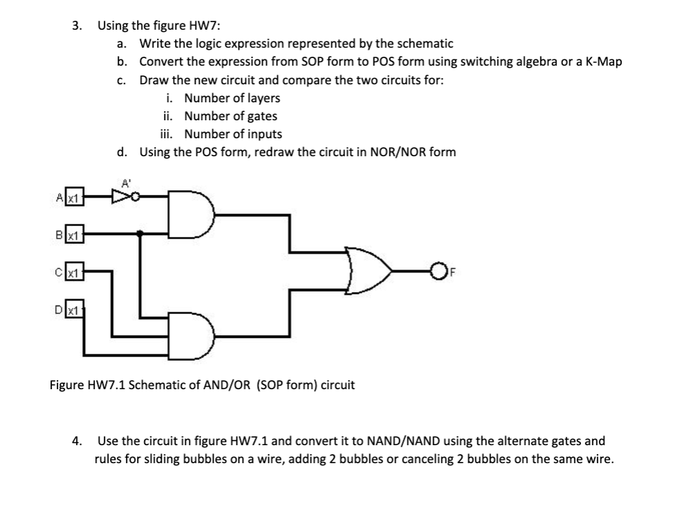
3. D x1 Using the figure HW7: a. Write the logic expression represented by the schematic b. Convert the expression from SOP form to POS form using switching algebra or a K-Map Draw the new circuit and compare the two circuits for: C. i. Number of layers ii. Number of gates iii. Number of inputs d. Using the POS form, redraw the circuit in NOR/NOR form Figure HW7.1 Schematic of AND/OR (SOP form) circuit 4. Use the circuit in figure HW7.1 and convert it to NAND/NAND using the alternate gates and rules for sliding bubbles on a wire, adding 2 bubbles or canceling 2 bubbles on the same wire. 3. D x1 Using the figure HW7: a. Write the logic expression represented by the schematic b. Convert the expression from SOP form to POS form using switching algebra or a K-Map Draw the new circuit and compare the two circuits for: C. i. Number of layers ii. Number of gates iii. Number of inputs d. Using the POS form, redraw the circuit in NOR/NOR form Figure HW7.1 Schematic of AND/OR (SOP form) circuit 4. Use the circuit in figure HW7.1 and convert it to NAND/NAND using the alternate gates and rules for sliding bubbles on a wire, adding 2 bubbles or canceling 2 bubbles on the same wire.
Step by Step Solution
There are 3 Steps involved in it
a The logic expression represented by the schematic in Figure HW71 is Ax1 AND Bx1 OR Cx1 AND D x1 b ... View full answer

Get step-by-step solutions from verified subject matter experts