

Question: 3. Differential pair with diode-connected loads: Consider the unity gain buffer amplifier shown below. The goal of this design is to achieve a DC gain
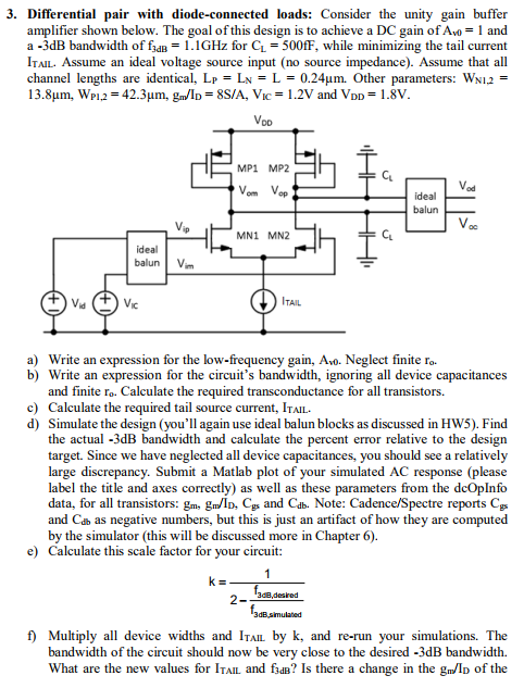
3. Differential pair with diode-connected loads: Consider the unity gain buffer amplifier shown below. The goal of this design is to achieve a DC gain of A+0-1 and a -3dB bandwidth of fa1.1GHz for CL 500fF, while minimizing the tail current ITAIL. Assume an ideal voltage source input (no source impedance). Assume that all channel lengths are identical, LP-LN-L = 0.24m. Other parameters: WNI,2 = 13.8m, Wp1.2 = 42.3m, grn/ID= 8S/A VIC = 1.2V and VDD = 1.8V OD MP1 MP2 CL ideal balun MN1 MN2 ideal balun V a) Write an expression for the low-frequency gain, Ao. Neglect finite ro b) Write an expression for the circuit's bandwidth, ignoring all device capacitances and finite ro. Calculate the required transconductance for all transistors. c) Calculate the required tail source current, ITAIL d) Simulate the design (you'll again use ideal balun blocks as discussed in HW5). Find the actual -3dB bandwidth and calculate the percent error relative to the design target. Since we have neglected all device capacitances, you should see a relatively large discrepancy. Submit a Matlab plot of your simulated AC response (please label the title and axes correctly) as well as these parameters from the deOplnfo data, for all transistors: gm, gm/D, Cgs and Cdb. Note: Cadence/Spectre reports Cs and Cdb as negative numbers, but this is just an artifact of how they are computed by the simulator (this will be discussed more in Chapter 6). Calculate this scale factor for your circuit: e) f) Multiply all device widths and ITAIL by k, and re-run your simulations. The bandwidth of the circuit should now be very close to the desired -3dB bandwidth. What are the new values for ITAIL and fdB? Is there a change in the gm/Io of the 3. Differential pair with diode-connected loads: Consider the unity gain buffer amplifier shown below. The goal of this design is to achieve a DC gain of A+0-1 and a -3dB bandwidth of fa1.1GHz for CL 500fF, while minimizing the tail current ITAIL. Assume an ideal voltage source input (no source impedance). Assume that all channel lengths are identical, LP-LN-L = 0.24m. Other parameters: WNI,2 = 13.8m, Wp1.2 = 42.3m, grn/ID= 8S/A VIC = 1.2V and VDD = 1.8V OD MP1 MP2 CL ideal balun MN1 MN2 ideal balun V a) Write an expression for the low-frequency gain, Ao. Neglect finite ro b) Write an expression for the circuit's bandwidth, ignoring all device capacitances and finite ro. Calculate the required transconductance for all transistors. c) Calculate the required tail source current, ITAIL d) Simulate the design (you'll again use ideal balun blocks as discussed in HW5). Find the actual -3dB bandwidth and calculate the percent error relative to the design target. Since we have neglected all device capacitances, you should see a relatively large discrepancy. Submit a Matlab plot of your simulated AC response (please label the title and axes correctly) as well as these parameters from the deOplnfo data, for all transistors: gm, gm/D, Cgs and Cdb. Note: Cadence/Spectre reports Cs and Cdb as negative numbers, but this is just an artifact of how they are computed by the simulator (this will be discussed more in Chapter 6). Calculate this scale factor for your circuit: e) f) Multiply all device widths and ITAIL by k, and re-run your simulations. The bandwidth of the circuit should now be very close to the desired -3dB bandwidth. What are the new values for ITAIL and fdB? Is there a change in the gm/Io of the
Step by Step Solution
There are 3 Steps involved in it

Get step-by-step solutions from verified subject matter experts