

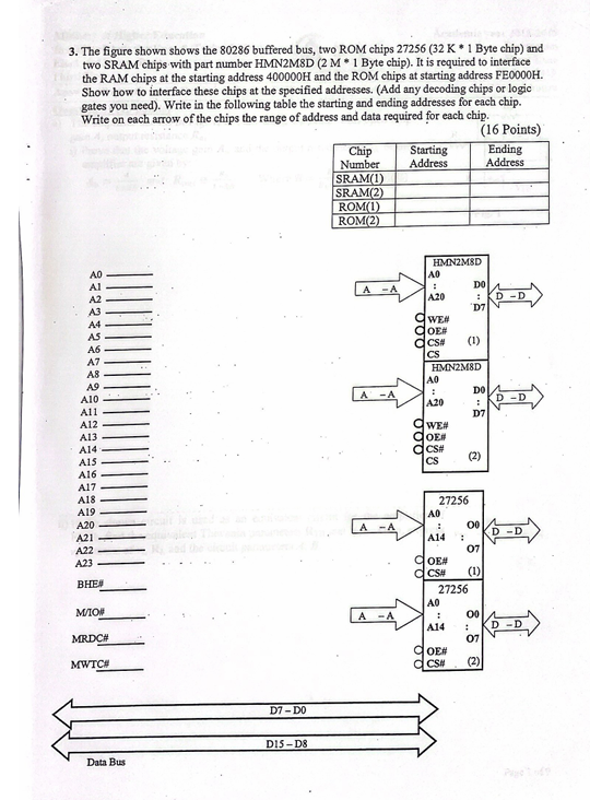
Question: 3 . The figure shown shows the 8 0 2 8 6 buffered bus, two ROM chips 2 7 2 5 6 ( 3 2
The figure shown shows the buffered bus, two ROM chips K Byte chip and two SRAM chips with part number HMNMD M Byte chip It is required to interface the RAM chips at the starting address H and the ROM chips at starting address FEH Show how to interface these chips at the specified addresses. Add any decoding chips or logic gates you need Write in the following table the starting and ending addresses for each chip. Write on each arrow of the chips the range of address and data required for each chip.
BHE
MO
MRDC#
MWTC#
Step by Step Solution
There are 3 Steps involved in it
1 Expert Approved Answer
Step: 1 Unlock

Question Has Been Solved by an Expert!
Get step-by-step solutions from verified subject matter experts
Step: 2 Unlock
Step: 3 Unlock