

Question: 3. The following schematic implements some logic function. The inverters at the input have a size of a-1 D Out1 D Out2 CL1 CL2
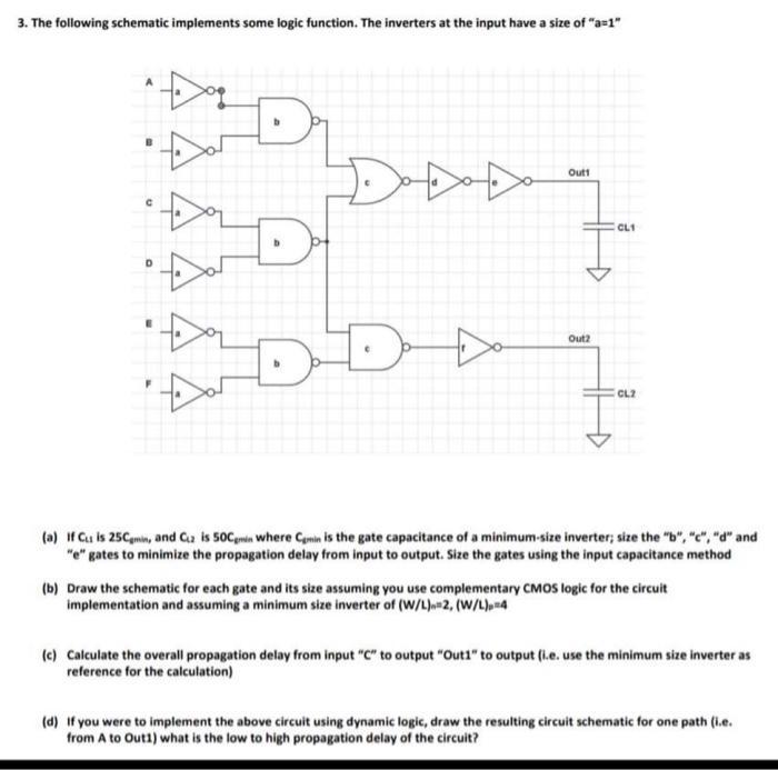
3. The following schematic implements some logic function. The inverters at the input have a size of "a-1" D Out1 D Out2 CL1 CL2 (a) If Cu is 25Cmin, and C is 50Cmin where Camin is the gate capacitance of a minimum-size inverter; size the "b", "c", "d" and "e" gates to minimize the propagation delay from input to output. Size the gates using the input capacitance method (b) Draw the schematic for each gate and its size assuming you use complementary CMOS logic for the circuit implementation and assuming a minimum size inverter of (W/L)-2, (W/L)=4 (c) Calculate the overall propagation delay from input "C" to output "Out1" to output (i.e. use the minimum size inverter as reference for the calculation) (d) If you were to implement the above circuit using dynamic logic, draw the resulting circuit schematic for one path (i.e. from A to Out1) what is the low to high propagation delay of the circuit?
Step by Step Solution
3.50 Rating (153 Votes )
There are 3 Steps involved in it

Get step-by-step solutions from verified subject matter experts