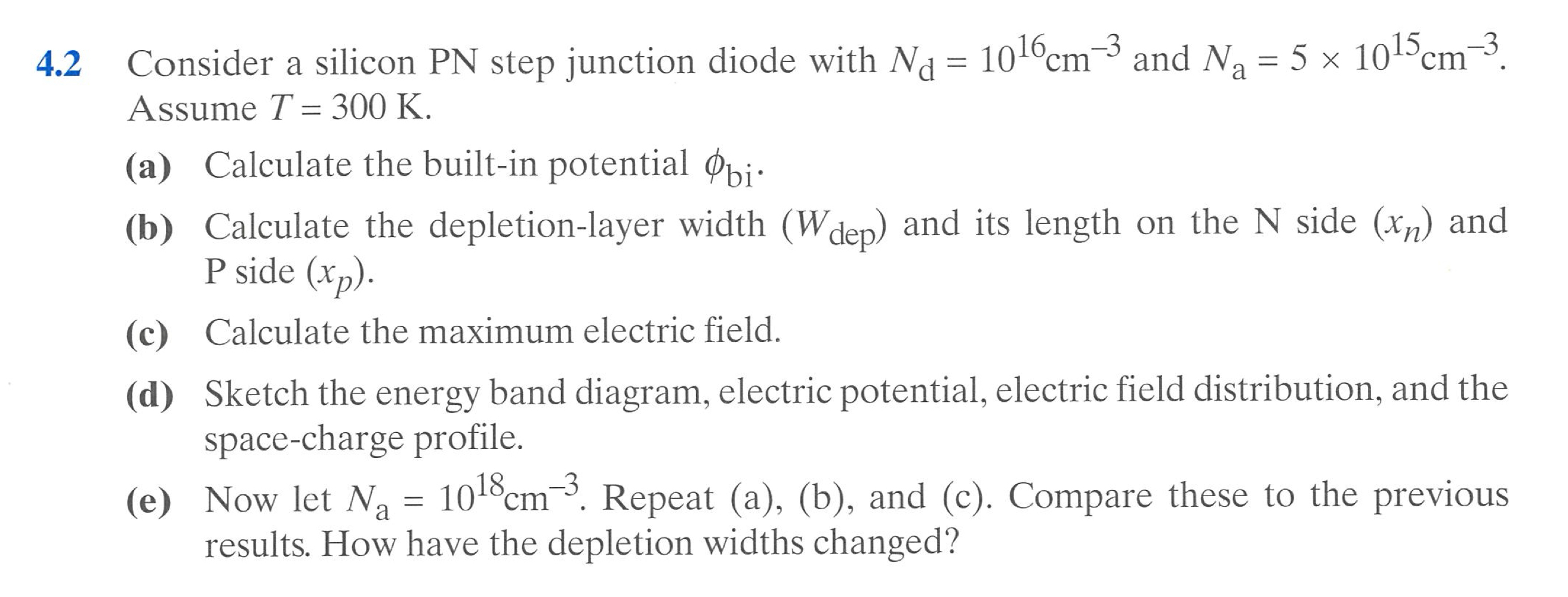
Question: 4 . 2 Consider a silicon PN step junction diode with N d = 1 0 1 6 c m - 3 and N a
Consider a silicon PN step junction diode with and Assume
a Calculate the builtin potential
b Calculate the depletionlayer width and its length on the N side and side
c Calculate the maximum electric field.
d Sketch the energy band diagram, electric potential, electric field distribution, and the spacecharge profile.
e Now let Repeat ab and c Compare these to the previous results. How have the depletion widths changed?

Step by Step Solution
There are 3 Steps involved in it
1 Expert Approved Answer
Step: 1 Unlock


Question Has Been Solved by an Expert!
Get step-by-step solutions from verified subject matter experts
Step: 2 Unlock
Step: 3 Unlock


