

Question: 4. A TLC1549 10-bit ADC chip using SPI communication with the USCl_A0 module is to be used in an application. The timing diagram to be
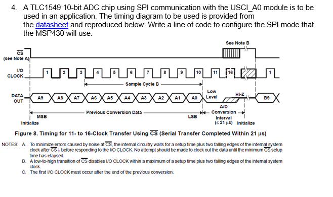
4. A TLC1549 10-bit ADC chip using SPI communication with the USCl_A0 module is to be used in an application. The timing diagram to be used is provided from the datasheet and reproduced below. Write a line of code to configure the SPI mode that the MSP430 will use. Figure 8. Timing for 11- to 16-Clock Transfer Using CS (Serial Transfer Completed Within 21s ) OTES: A. To minimize errors caused by noise at CS, the internal circuitry waits for a setup time plus two falling edges of the intemal system clock after CS before responding to the vO CLOCK. No attempt should be made to clock out the data until the minimum CS setup time has elapsed. B. A low-to-high transition of CS disables vO CLOCK within a maximum of a setup time plus two falling edges of the intemal system clock. C. The first vO CLOCK must occur after the end of the previous conversion
Step by Step Solution
There are 3 Steps involved in it

Get step-by-step solutions from verified subject matter experts