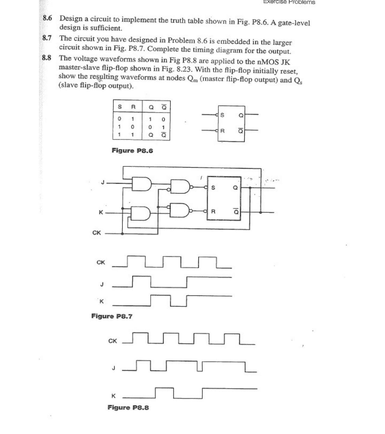
Question: 8 . 6 Design a circuit to implement the truth table shown in Fig. P 8 . 6 . A gate - level design is
Design a circuit to implement the truth table shown in Fig. P A gatelevel design is sufficient.
The circuit you have designed in Problem is embedded in the larger circuit shown in Fig. P Complete the timing diagram for the output.
The voltage waveforms shown in Fig P are applied to the nMOS JK masterslave flipflop shown in Fig. With the flipflop initially reset, show the resulting waveforms at nodes master flipflop output and slave flipflop output
table

Step by Step Solution
There are 3 Steps involved in it
1 Expert Approved Answer
Step: 1 Unlock


Question Has Been Solved by an Expert!
Get step-by-step solutions from verified subject matter experts
Step: 2 Unlock
Step: 3 Unlock


