

Question: 9 . 9 Show a step by step simulink model build of a buck - boost voltage regulator. The buck - boost converter of Fig.
Show a step by step simulink model build of a buckboost voltage regulator. The buckboost converter of Fig. operates in the continu
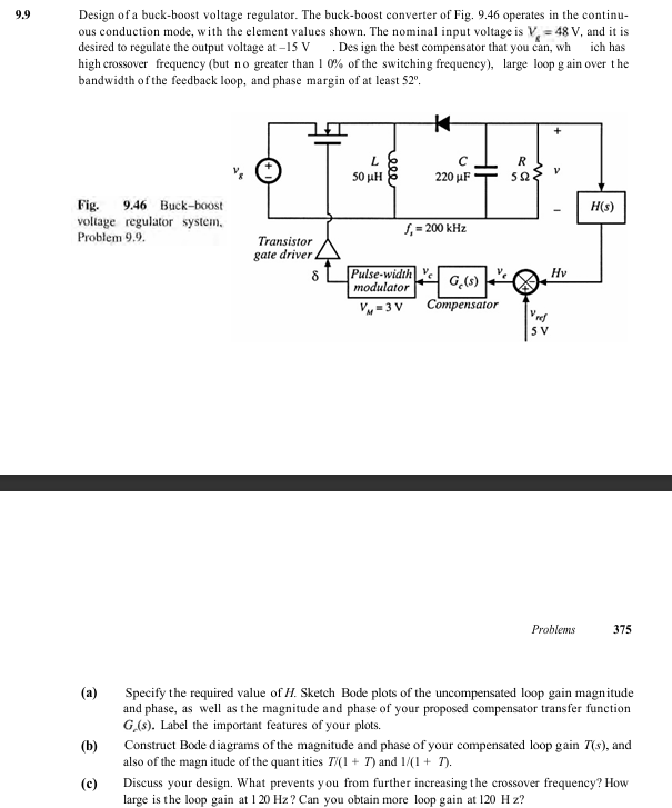
ous conduction mode, with the element values shown. The nominal input voltage is VsV and it is desired to regulate the output voltage at V Des ign the best compensator that you can, wh ich has
high crossover frequency but no greater than of the switching frequency large loop g ain over the bandwidth of the feedback loop, and phase margin of at least @
Fig. Buckboost
voltage regulator system.
Problem
show the model responses for the following problems:
a Specify the required value of H Sketch Bode plots of the uncompensated loop gain magnitude and phase, as well as the magnitude and phase of your proposed compensator transfer function
Gcs Label the important features of your plots.
b Construct Bode diagrams of the magnitude and phase of your compensated loop gain Ts and also of the magn itude of the quant ities TT and T
c Discuss your design. What prevents y ou from further increasing the crossover frequency? How large is the loop gain at Hz Can you obtain more loop gain at Hz
Step by Step Solution
There are 3 Steps involved in it
1 Expert Approved Answer
Step: 1 Unlock

Question Has Been Solved by an Expert!
Get step-by-step solutions from verified subject matter experts
Step: 2 Unlock
Step: 3 Unlock