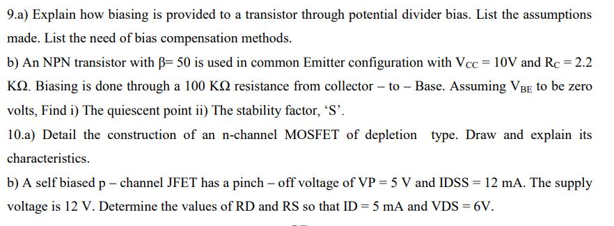
Question: 9.a) Explain how biasing is provided to a transistor through potential divider bias. List the assumptions made. List the need of bias compensation methods.

9.a) Explain how biasing is provided to a transistor through potential divider bias. List the assumptions made. List the need of bias compensation methods. b) An NPN transistor with = 50 is used in common Emitter configuration with Vcc = 10V and Rc = 2.2 KQ. Biasing is done through a 100 KQ resistance from collector - to - Base. Assuming VBE to be zero volts, Find i) The quiescent point ii) The stability factor, 'S'. 10.a) Detail the construction of an n-channel MOSFET of depletion type. Draw and explain its characteristics. b) A self biased p-channel JFET has a pinch-off voltage of VP = 5 V and IDSS = 12 mA. The supply voltage is 12 V. Determine the values of RD and RS so that ID = 5 mA and VDS = 6V.
Step by Step Solution
There are 3 Steps involved in it

Get step-by-step solutions from verified subject matter experts


