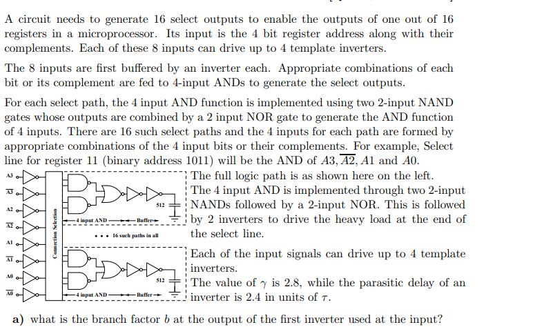
Question: A circuit needs to generate 16 select outputs to enable the outputs of one out of 16 registers in a microprocessor. Its input is

![]()
![]()
![]()
![]()
A circuit needs to generate 16 select outputs to enable the outputs of one out of 16 registers in a microprocessor. Its input is the 4 bit register address along with their complements. Each of these 8 inputs can drive up to 4 template inverters. The 8 inputs are first buffered by an inverter each. Appropriate combinations of each bit or its complement are fed to 4-input ANDs to generate the select outputs. For each select path, the 4 input AND function is implemented using two 2-input NAND gates whose outputs are combined by a 2 input NOR gate to generate the AND function of 4 inputs. There are 16 such select paths and the 4 inputs for each path are formed by appropriate combinations of the 4 input bits or their complements. For example, Select line for register 11 (binary address 1011) will be the AND of A3, A2, A1 and 40. A3 - A3 2 A2 21 AI AI 9 19 AO Connection Selection 200 BD -4 input AND-Buffer ... 16 such paths in all 512 4 imput AND Buffer 512 The value of y is 2.8, while the parasitic delay of an inverter is 2.4 in units of 7. a) what is the branch factor b at the output of the first inverter used at the input? The full logic path is as shown here on the left. The 4 input AND is implemented through two 2-input NANDs followed by a 2-input NOR. This is followed by 2 inverters to drive the heavy load at the end of the select line. Each of the input signals can drive up to 4 template inverters. b) Compute the optimum stage effort f for this circuit if the final output has to drive a load equivalent to 512 template inverters. c) Compute the input capacitance in units of the input capacitance of the template inverter for each stage. d) Compute the n and p channel transistor geometry size for each stage. e) Find the total delay of the logic path in units of 7.
Step by Step Solution
3.43 Rating (156 Votes )
There are 3 Steps involved in it
The detailed ... View full answer

Get step-by-step solutions from verified subject matter experts


