

Question: A quiz for CPU structrue and function. NO SPAM PLZ! Look at the following (incomplete) diagram of the Hack CPU. Look at the wire pointed
A quiz for CPU structrue and function. NO SPAM PLZ!
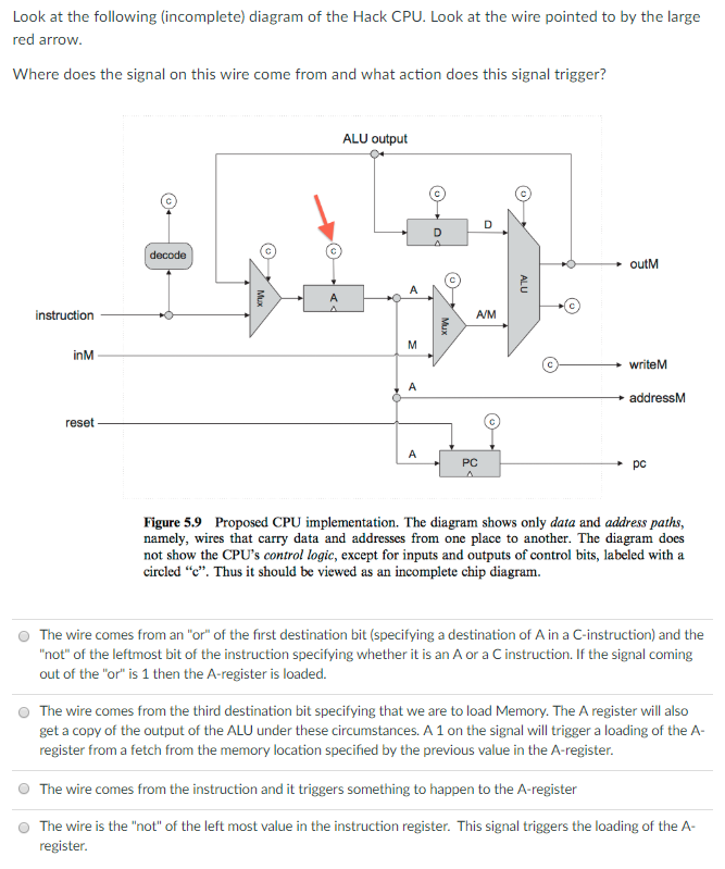
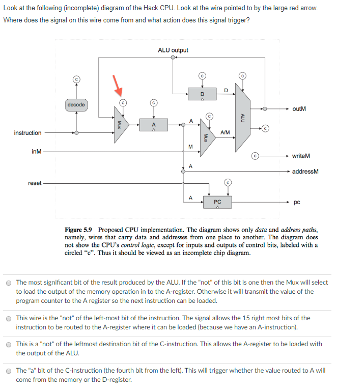
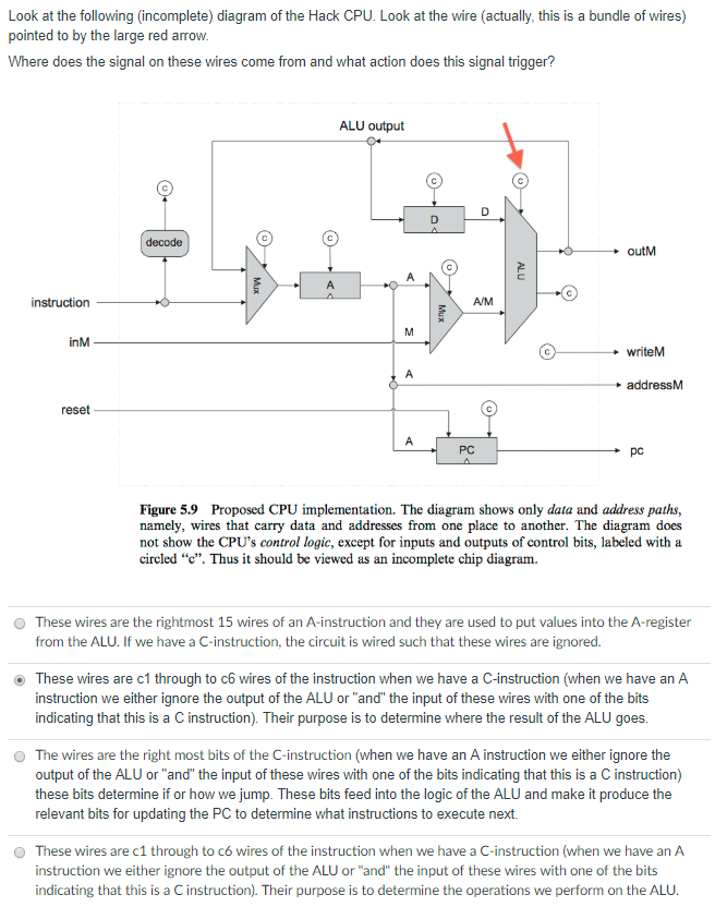
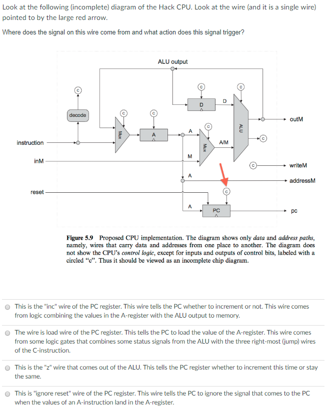
Look at the following (incomplete) diagram of the Hack CPU. Look at the wire pointed to by the large red arrOw Where does the signal on this wire come from and what action does this signal trigger? ALU output outM A/M inM writeM addressM reset PC Figure 5.9 Proposed CPU implementation. The diagram shows only data and address paths, namely, wires that carry data and addresses from one place to another. The diagram does not show the CPU's control logic, except for inputs and outputs of control bits, labeled with a circled "c". Thus it should be viewed as an incomplete chip diagram. O The wire comes from an "or" of the first destination bit (specifying a destination of A in a C-instruction) and the "not" of the leftmost bit of the instruction specifying whether it is an A or a C instruction. If the signal coming out of the "or" is 1 then the A-register is loaded. The wire comes from the third destination bit specifying that we are to load Memory. The A register will also get a copy of the output of the ALU under these circumstances. A 1 on the signal will trigger a loading of the A register from a fetch from the memory location specified by the previous value in the A-register O O The wire comes from the instruction and it triggers something to happen to the A-register The wire is the "not" of the left most value in the instruction register. This signal triggers the loading of the A register O Look at the following (incomplete) diagram of the Hack CPU. Look at the wire pointed to by the large red arrOw Where does the signal on this wire come from and what action does this signal trigger? ALU output outM A/M inM writeM addressM reset PC Figure 5.9 Proposed CPU implementation. The diagram shows only data and address paths, namely, wires that carry data and addresses from one place to another. The diagram does not show the CPU's control logic, except for inputs and outputs of control bits, labeled with a circled "c". Thus it should be viewed as an incomplete chip diagram. O The wire comes from an "or" of the first destination bit (specifying a destination of A in a C-instruction) and the "not" of the leftmost bit of the instruction specifying whether it is an A or a C instruction. If the signal coming out of the "or" is 1 then the A-register is loaded. The wire comes from the third destination bit specifying that we are to load Memory. The A register will also get a copy of the output of the ALU under these circumstances. A 1 on the signal will trigger a loading of the A register from a fetch from the memory location specified by the previous value in the A-register O O The wire comes from the instruction and it triggers something to happen to the A-register The wire is the "not" of the left most value in the instruction register. This signal triggers the loading of the A register O
Step by Step Solution
There are 3 Steps involved in it

Get step-by-step solutions from verified subject matter experts