

Question: a. Write the Verilog prototype for a 2-to-1 multiplexer, with chip-enable input (CE), using structural design approach and active-high tri-state buffers. Assume that the
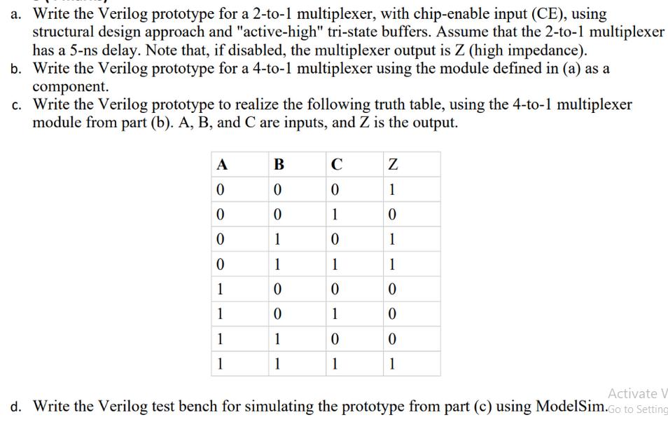
a. Write the Verilog prototype for a 2-to-1 multiplexer, with chip-enable input (CE), using structural design approach and "active-high" tri-state buffers. Assume that the 2-to-1 multiplexer has a 5-ns delay. Note that, if disabled, the multiplexer output is Z (high impedance). b. Write the Verilog prototype for a 4-to-1 multiplexer using the module defined in (a) as a component. c. Write the Verilog prototype to realize the following truth table, using the 4-to-1 multiplexer module from part (b). A, B, and C are inputs, and Z is the output. A B C Z 0 0 0 1 0 0 1 0 0 1 0 1 0 1 1 1 1 0 0 0 1 0 1 0 1 1 0 0 1 1 1 1 Activate V d. Write the Verilog test bench for simulating the prototype from part (c) using ModelSim. Go to Setting
Step by Step Solution
There are 3 Steps involved in it
a Heres the Verilog code for a 2to1 multiplexer with chipenable input using activehigh tristate buff... View full answer

Get step-by-step solutions from verified subject matter experts