

Question: Add logic and data paths to the single cycle LC - 3 implementation to allow for the following instructions: a . BR b . JMP
Add logic and data paths to the single cycle LC implementation to allow for the following instructions:
a BR
b JMP
c JSR
d JSRR
e RET For each of the instructions, explain in words how the data flows through the data path.
Assume the following timing data for the various components used in the single cycle and pipelined implementations of the LC
Element Delay ps Register clock to Q Register setup Multiplexer ALUAdder Memory read or write Signzero extension Register file read Register file setup
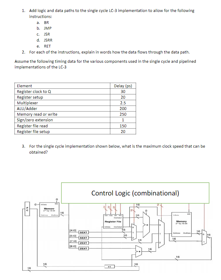
For the single cycle implementation shown below, what is the maximum clock speed that can be obtained?
For the pipelined implementation below, what is the minimum clock cycle time required for each
stage, namely:
a Data fetch stage
b Data decode stage
c Register read stage
d ALU operation stage
e Memory readwrite stage
f Register writeback stage
What's the max clock speed for this pipelined implementation?
If you could reduce the delay for one component, which would you choose? How much would you
reduce the delay? hint: at some point, reducing the delay in one component doesn't help reduce the
clock period
If you could speed up two componenets, which two? How much would you reduce their delays?
LC Pipelined Implementation
Please use the included diagram and element delay timing chart in your answer please. Thank you so much!
Step by Step Solution
There are 3 Steps involved in it
1 Expert Approved Answer
Step: 1 Unlock

Question Has Been Solved by an Expert!
Get step-by-step solutions from verified subject matter experts
Step: 2 Unlock
Step: 3 Unlock