

Question: Answer the question 2-a) Briefly describe (i) the basic working principles of a Dc-Dc boost converter circuit and subsequently (ii) derive an expression for the
Answer the question
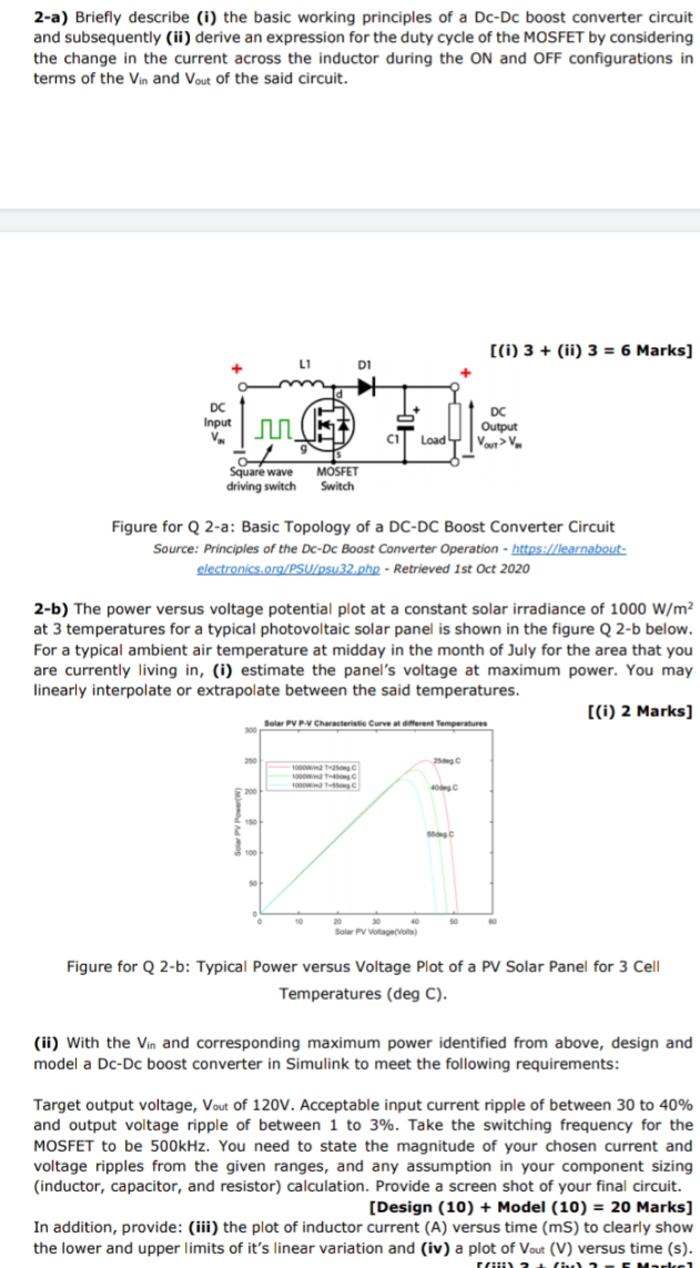
2-a) Briefly describe (i) the basic working principles of a Dc-Dc boost converter circuit and subsequently (ii) derive an expression for the duty cycle of the MOSFET by considering the change in the current across the inductor during the ON and OFF configurations in terms of the Vin and Vout of the said circuit. [(i) 3 + (ii) 3 = 6 Marks] L1 D1 DC DC Input Output Load VOUT> V. Square wave MOSFET driving switch Switch Figure for Q 2-a: Basic Topology of a DC-DC Boost Converter Circuit Source: Principles of the DC-DC Boost Converter Operation - https://learnabout- electronics.org/PSU/psu.32.php - Retrieved Ist Oct 2020 2-b) The power versus voltage potential plot at a constant solar irradiance of 1000 W/m at 3 temperatures for a typical photovoltaic solar panel is shown in the figure Q 2-b below. For a typical ambient air temperature at midday in the month of July for the area that you are currently living in, (i) estimate the panel's voltage at maximum power. You may linearly interpolate or extrapolate between the said temperatures. [(i) 2 Marks] Solar PV P.V Characteristic Curve at different Ten 25dag C 150 PV 100 Figure for Q 2-b: Typical Power versus Voltage Plot of a PV Solar Panel for 3 Cell Temperatures (deg C). (ii) With the Vin and corresponding maximum power identified from above, design and model a Dc-Dc boost converter in Simulink to meet the following requirements: Target output voltage, Vout of 120V. Acceptable input current ripple of between 30 to 40% and output voltage ripple of between 1 to 3%. Take the switching frequency for the MOSFET to be 500kHz. You need to state the magnitude of your chosen current and voltage ripples from the given ranges, and any assumption in your component sizing (inductor, capacitor, and resistor) calculation. Provide a screen shot of your final circuit. [Design (10) + Model (10) = 20 Marks] In addition, provide: (iii) the plot of inductor current (A) versus time (mS) to clearly show the lower and upper limits of it's linear variation and (iv) a plot of Vout (V) versus time (s)
Step by Step Solution
There are 3 Steps involved in it

Get step-by-step solutions from verified subject matter experts