

Question: can you please solve part (e) and (f)? Problem1 The logic for a Full-Adder (FA) (from the lecture notes) is shown in the figure below.
can you please solve part (e) and (f)?
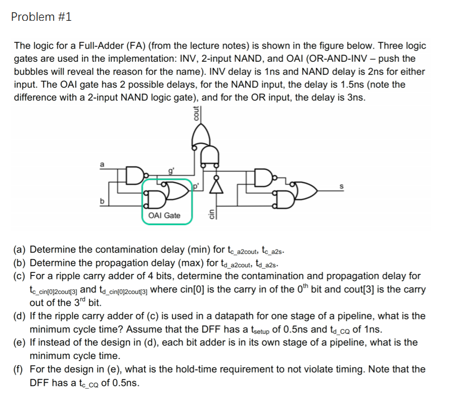
Problem1 The logic for a Full-Adder (FA) (from the lecture notes) is shown in the figure below. Three logic gates are used in the implementation: INV, 2-input NAND, and OAI (OR-AND-INV - push the bubbles will reveal the reason for the name). INV delay is 1ns and NAND delay is 2ns for either input. The OAl gate has 2 possible delays, for the NAND input, the delay is 1.5ns (note the difference with a 2-input NAND logic gate), and for the OR input, the delay is 3ns. OAl Gate (a) Determine the contamination delay (min) for te a2cout, tc a2s- (b) Determine the propagation delay (max) for td a2cout, td a2s. (c) For a ripple carry adder of 4 bits, determine the contamination and propagation delay for te cin(op2coutsy and to cin(op2coutsy where cin(O] is the carry in of the oth bit and cout 3] is the carry (d) If the ripple carry adder of (c) is used in a datapath for one stage of a pipeline, what is the (e) If instead of the design in (d), each bit adder is in its own stage of a pipeline, what is the (f) For the design in (e), what is the hold-time requirement to not violate timing. Note that the out of the 3rd bit. minimum cycle time? Assume that the DFF has a tsetup of 0.5ns and td_co of 1ns. minimum cycle time. DFF has a te co of 0.5ns
Step by Step Solution
There are 3 Steps involved in it

Get step-by-step solutions from verified subject matter experts