

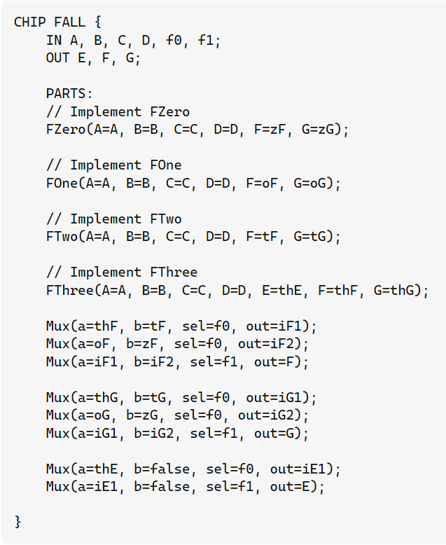
Question: CHIP FALL { IN A , B , C , D , f 0 , f 1 ;PARTS:FZero ( A = A , B =
CHIP FALL IN A B C D f f;PARTS:FZeroAA BB CC DD FzF GzG;FOneAA BB CC DD FoF GoG;FTwoAA BB CC DD FtF GtG;FThreeAA BB CC DD EthE, FthF GthG;MuxaoF bzF self outiF;MuxathG btG self outiG;MuxaiG biG self outG;MuxaiE bfalse, self outE;
IN A B C D f f;
OUT E F G;
PARTS:
Implement FZero
FZeroAA BB CC DD FzF GzG;
Implement FOne
FOneAA BB CC DD FoF GoG;
Implement FTwo
FTwoAA BB CC DD FtF GtG;
Implement FThree
FThreeAA BB CC DD EthE, FthF GthG;
MuxathF btF self outiF;
MuxaoF bzF self outiF;
MuxaiF biF self outF;
MuxathG btG self outiG;
MuxaoG bzG self outiG;
MuxaiG biG self outG;
MuxathE, bfalse, self outiE;
MuxaiE bfalse, self outE;
Question:
As per nandtetris, Adapt the circuit FALL so that it can combine a sequence of operations defined by different values for f and f at each step, by enabling the outputs Ft and Gt of step t to be used feedback as the inputs for the next operation Ct and Dt for step t You should also add a further input Load to the chip which when Load will enable you to load new inputs to Ct and Dt and when set to sets Ct Ft and Dt Gt The Load input will allow you to manually set the values of C and D at the start and during the sequence if required. Call this chip FSEQ.
You must only use the builtin AND, NAND, OR NOR, NOT, Mux, DMux,XOR or DFF chips.
Step by Step Solution
There are 3 Steps involved in it
1 Expert Approved Answer
Step: 1 Unlock

Question Has Been Solved by an Expert!
Get step-by-step solutions from verified subject matter experts
Step: 2 Unlock
Step: 3 Unlock