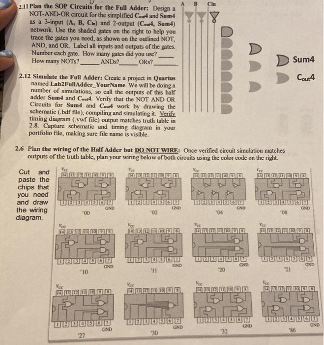
Question: Cin Do 2.11 Plan the SOP Circuits for the Full Adder: Design a NOT-AND-OR circuit for the simplified Cow4 and Sum4 as a 3-input (A,

Cin Do 2.11 Plan the SOP Circuits for the Full Adder: Design a NOT-AND-OR circuit for the simplified Cow4 and Sum4 as a 3-input (A, B, Cin) and 2-output (Cou4, Sum4) network. Use the shaded gates on the right to help you trace the gates you need, as shown on the outlined NOT, AND, and OR. Label all inputs and outputs of the gates. Number each gate. How many gates did you use? How many NOTS? ANDs? ORS? Sum4 Cout4 2.12 Simulate the Full Adder: Create a project in Quartus named Lab2FullAdder_Your Name. We will be doing a number of simulations, so call the outputs of this half adder Sum4 and Cut4. Verify that the NOT AND OR Circuits for Sum4 and Cou4 work by drawing the schematic (.bdf file), compiling and simulating it. Verify timing diagram (vwf file) output matches truth table in 2.8. Capture schematic and timing diagram in your portfolio file, making sure file name is visible. 2.6 Plan the wiring of the Half Adder but DO NOT WIRE: Once verified circuit simulation matches outputs of the truth table, plan your wiring below of both circuits using the color code on the right. Cut and Ver Yee 10300 paste the 2. chips that you need and draw De the wiring "00 02 "04 '08 diagram Voc Vec 103 D BUD 0 GND GND OND Voc Ver GND OND GND OND 10 '11 20 Voc Voe 10 m Ver 8 PA EDZI GND 27 UIRIE 32 OND OND GND "86 30
Step by Step Solution
There are 3 Steps involved in it

Get step-by-step solutions from verified subject matter experts


