

Question: Circuit below represents structural design of 4 bits binary up counter Carry3 Cout A S Sum3 HA V Rst D Q B Cik Carry2
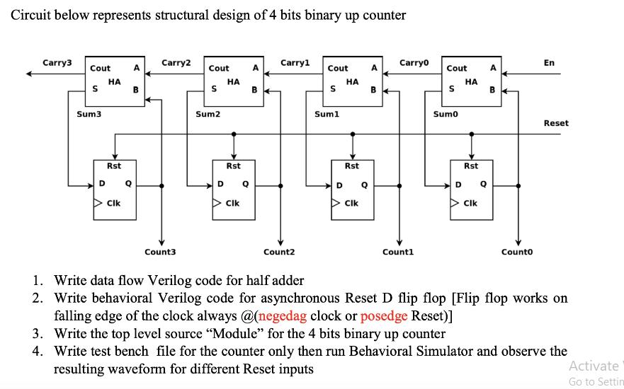
Circuit below represents structural design of 4 bits binary up counter Carry3 Cout A S Sum3 HA V Rst D Q B Cik Carry2 Count3 Cout S Sum2 HA V Rst D Q CIK A B Carry1 Count2 Cout S Sum1 D HA Rst CIK A B Carry0 Countl Cout S Sumo D HA Rst Cik Q A B Counto En Reset 1. Write data flow Verilog code for half adder 2. Write behavioral Verilog code for asynchronous Reset D flip flop [Flip flop works on falling edge of the clock always @(negedag clock or posedge Reset)] 3. Write the top level source "Module" for the 4 bits binary up counter 4. Write test bench file for the counter only then run Behavioral Simulator and observe the resulting waveform for different Reset inputs Activate Go to Settin
Step by Step Solution
There are 3 Steps involved in it

Get step-by-step solutions from verified subject matter experts