

Question: COMP 3033 Assignment 2 SPRING 2019 DUE 2/26/2019 Del NO COPYING. PLEASE WRITE NEATLY IN THE ORDER OF QUESTIONS. ALL STEPS MUST BE SHOWN TO
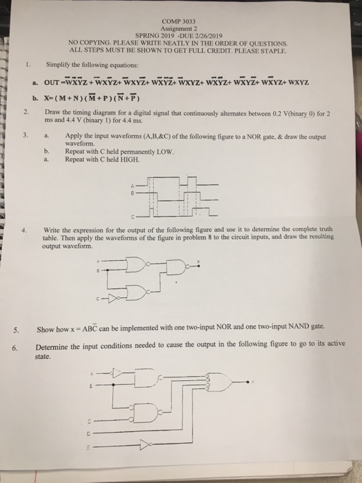
COMP 3033 Assignment 2 SPRING 2019 DUE 2/26/2019 Del NO COPYING. PLEASE WRITE NEATLY IN THE ORDER OF QUESTIONS. ALL STEPS MUST BE SHOWN TO GET FULL CREDIT. PLEASE STAPLE 1 Simplify the following equations: b. X (M+N) (M+P) (N+P) 2. Draw the timing diagram for a digital signal that continuously alternates between 0.2 V(binary 0) for 2 ms and 4.4 V (binary 1) for 4.4 ms. 3. a Apply the input waveforms (A,B,&C) of the following figure to a NOR gate, & draw the output waveform. b. Repeat with C held permanently LOW a. Repeat with C held HIGH. 4. Write the expression for the output of the following figure and use it to determine the complete truth table. Then apply the waveforms of the figure in problem 8 to the circuit inputs, and draw the resulting output waveform 5. Show how x ABC can be implemented with one two-input NOR and one two-input NAND gate. 6. Determine the input conditions needed to cause the output in the following figure to go to its active state
Step by Step Solution
There are 3 Steps involved in it

Get step-by-step solutions from verified subject matter experts