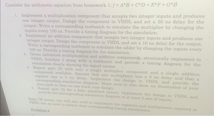
Question: Consider the arithmetic equation from homework 1:f=AB+CD+EF+GH 1. Implement a multiplication component that accepts two integer inputs and produces one integer output. Design the component

Consider the arithmetic equation from homework 1:f=AB+CD+EF+GH 1. Implement a multiplication component that accepts two integer inputs and produces one integer output. Design the component in VHDL and set a 50ns delay for the output. Write a corresponding testbench to simulate the multiplier by changing the inputs every 100ns. Provide a timing diagram for the simulation. 2. Implement an addition component that accepts two integer inputs and produces one integer output. Design the component in VHDL and set a 10 ns delay for the output. Write a corresponding testbench to simulate the adder by changing the inputs every 100 ns. Provide a timing diagram for the simulation. 3. Given unlimited multipliention and addition componentis, structurally implement in. VHDL function f along with a testbench and provide a timing diagram for the simulution clearly showing the signal names. 4. Repeat part (3) with only a single multiplior component and a single addition component available. Assume that any multiplexer has a 5na deliky and that a reginter has a 3mn delay. Implement the design in VHDL and provide the correnponding simulation dingram. Make sure to also ahow an illustration of your 6. Hepoat part, (3) for an frilly niok your design. Note: Of course, you will wino noed to implement the regiaters and multiplexern required in provide the correnponding simblined circuit, Implement the design in VHDL and VHDL but no need to sulbrit their corresponding timing simulntion. Broblem.2
Step by Step Solution
There are 3 Steps involved in it

Get step-by-step solutions from verified subject matter experts


