

Question: Consider the sequential circuit shown in the figure and assume that the outputs Q1, Q2 and Q3 are initially all reset to o logic state.
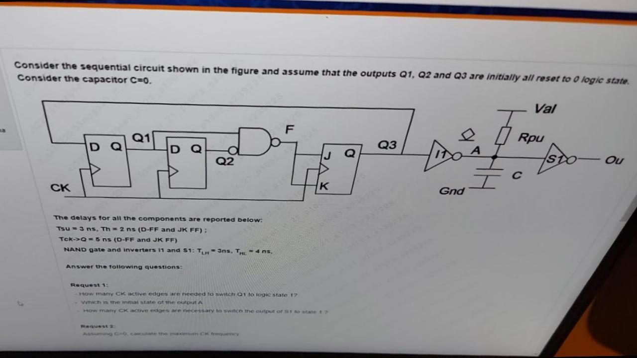
Consider the sequential circuit shown in the figure and assume that the outputs Q1, Q2 and Q3 are initially all reset to o logic state. Consider the capacitor C=0. Val F Q1 7 Q3 Rpu Q2 Ou CK K Gnd The delays for all the components are reported below: Tsuns. Th2 ns (D-FF and JK FF): Tek->Q-6 ns (D-FF and JK FF) NAND gate and inverters 11 and 51: TH-3ns. TAL = 4 ns. Answer the following questions: Request 1: How many CK active edges are needed to switch on to logic state 12 which is the inna state of the output A How many CK active edges are necessary to switch the output of state Consider the sequential circuit shown in the figure and assume that the outputs Q1, Q2 and Q3 are initially all reset to o logic state. Consider the capacitor C=0. Val F Q1 7 Q3 Rpu Q2 Ou CK K Gnd The delays for all the components are reported below: Tsuns. Th2 ns (D-FF and JK FF): Tek->Q-6 ns (D-FF and JK FF) NAND gate and inverters 11 and 51: TH-3ns. TAL = 4 ns. Answer the following questions: Request 1: How many CK active edges are needed to switch on to logic state 12 which is the inna state of the output A How many CK active edges are necessary to switch the output of state
Step by Step Solution
There are 3 Steps involved in it

Get step-by-step solutions from verified subject matter experts