

Question: Derive Equation 6 Space Vector Modulation (SVM) refers to a special switching sequence of the upper three power MOSFET s of a three-phase inverter. The
 Derive Equation 6
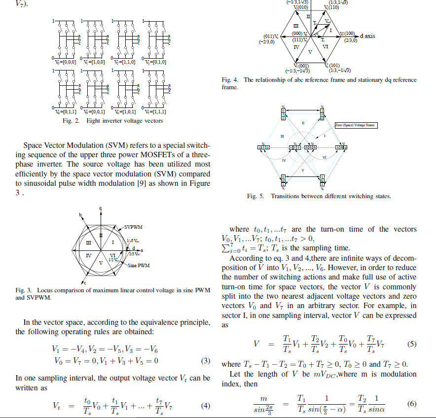
Space Vector Modulation (SVM) refers to a special switching sequence of the upper three power MOSFET s of a three-phase inverter. The source voltage has been utilized most efficiently by the space vector modulation (SVM) compared to sinusoidal pulse width modulation [9] as shown in Figure 3. In the vector space, according to the equivalence principle, the following operating rules are obtained: V1 = -V4, V_2 = -V_5, V_3 = - V_6 V_0 = V_7 = 0, V_1 + V_3 + V_5 = 0 In one sampling interval, the output voltage vector V_t can be written as V_t = t_0/T_s V_0 + t_1/T_s V_1 + ... + t_7/T_8 V_7 where t_0, t_1, ... t_7 are the turn-on time of the vectors V_0, V_1, .... V_7; t_0, t_1, ... t_7 > 0, sigma^7_i = 0 t_i = T_s; T_s is the sampling time. According to eq. 3 and 4, there are infinite ways of decomposition of V into V_1, V_2, ... V_6. However, in order to reduce the number of switching actions and make full use of active turn-on time for space vectors, the vector V is commonly split into the two nearest adjacent voltage vectors and zero vectors V_0 and V_7 in an arbitrary sector. For example, in sector I, in one sampling interval, vector V can be expressed as V = T_1/T_s V_1 + T_2/T_s V_2 + T_0/T_s V_0 + T_7/T_s V_7 where T_s - T_1 - T_2 = T_0 + T_7 greaterthanorequalto 0 and T_7 greaterthanorequalto 0. Let the length of V be mV_DC, where m is modulation index, then m/sin 2 pi/3 = T_1/T_s 1/sin(pi/3 - alpha) = T_2/T_s 1/sin alpha Space Vector Modulation (SVM) refers to a special switching sequence of the upper three power MOSFET s of a three-phase inverter. The source voltage has been utilized most efficiently by the space vector modulation (SVM) compared to sinusoidal pulse width modulation [9] as shown in Figure 3. In the vector space, according to the equivalence principle, the following operating rules are obtained: V1 = -V4, V_2 = -V_5, V_3 = - V_6 V_0 = V_7 = 0, V_1 + V_3 + V_5 = 0 In one sampling interval, the output voltage vector V_t can be written as V_t = t_0/T_s V_0 + t_1/T_s V_1 + ... + t_7/T_8 V_7 where t_0, t_1, ... t_7 are the turn-on time of the vectors V_0, V_1, .... V_7; t_0, t_1, ... t_7 > 0, sigma^7_i = 0 t_i = T_s; T_s is the sampling time. According to eq. 3 and 4, there are infinite ways of decomposition of V into V_1, V_2, ... V_6. However, in order to reduce the number of switching actions and make full use of active turn-on time for space vectors, the vector V is commonly split into the two nearest adjacent voltage vectors and zero vectors V_0 and V_7 in an arbitrary sector. For example, in sector I, in one sampling interval, vector V can be expressed as V = T_1/T_s V_1 + T_2/T_s V_2 + T_0/T_s V_0 + T_7/T_s V_7 where T_s - T_1 - T_2 = T_0 + T_7 greaterthanorequalto 0 and T_7 greaterthanorequalto 0. Let the length of V be mV_DC, where m is modulation index, then m/sin 2 pi/3 = T_1/T_s 1/sin(pi/3 - alpha) = T_2/T_s 1/sin alpha
Step by Step Solution
There are 3 Steps involved in it

Get step-by-step solutions from verified subject matter experts