

Question: Digital System Design Sequential Logic Design Assignment A successive approximation ADC achieves conversion of an analog signal Vin to an digital representation Dn - 1
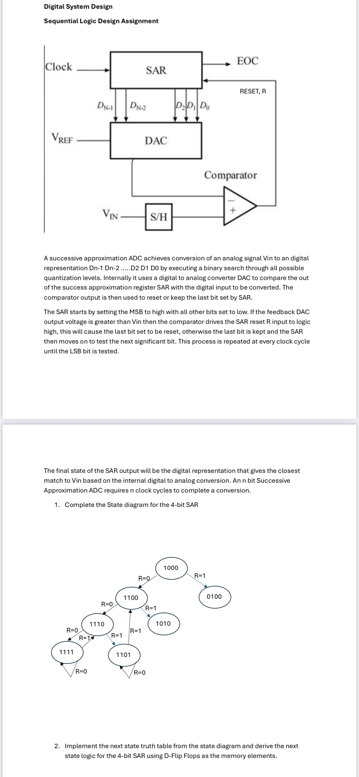
Digital System Design
Sequential Logic Design Assignment
A successive approximation ADC achieves conversion of an analog signal Vin to an digital representation Dn DnD D D by executing a binary search through all possible quantization levels. Internally it uses a digital to analog converter DAC to compare the out of the success approximation register SAR with the digital input to be converted. The comparator output is then used to reset or keep the last bit set by SAR.
The SAR starts by setting the MSB to high with all other bits set to low. If the feedback DAC output voltage is greater than Vin then the comparator drives the SAR reset input to logic high, this will cause the last bit set to be reset, otherwise the last bit is kept and the SAR then moves on to test the next significant bit. This process is repeated at every clock cycle until the LSB bit is tested.
The final state of the SAR output will be the digital representation that gives the closest match to Vin based on the internal digital to analog conversion. An n bit Successive Approximation ADC requires n clock cycles to complete a conversion.
Complete the State diagram for the bit SAR
Implement the next state truth table from the state diagram and derive the next state logic for the bit SAR using DFlip Flops as the memory elements.
Step by Step Solution
There are 3 Steps involved in it
1 Expert Approved Answer
Step: 1 Unlock

Question Has Been Solved by an Expert!
Get step-by-step solutions from verified subject matter experts
Step: 2 Unlock
Step: 3 Unlock