

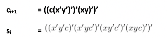
Question: Draw out the circuit for the full adder given the following NAND and NOT formatted versions of C_i+1 and S_i Also fill out this table
Draw out the circuit for the full adder given the following NAND and NOT formatted versions of C_i+1 and S_i
Also fill out this table for the delay and transistor count
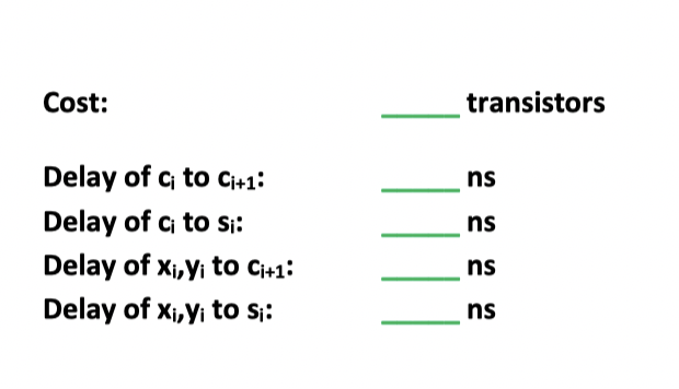
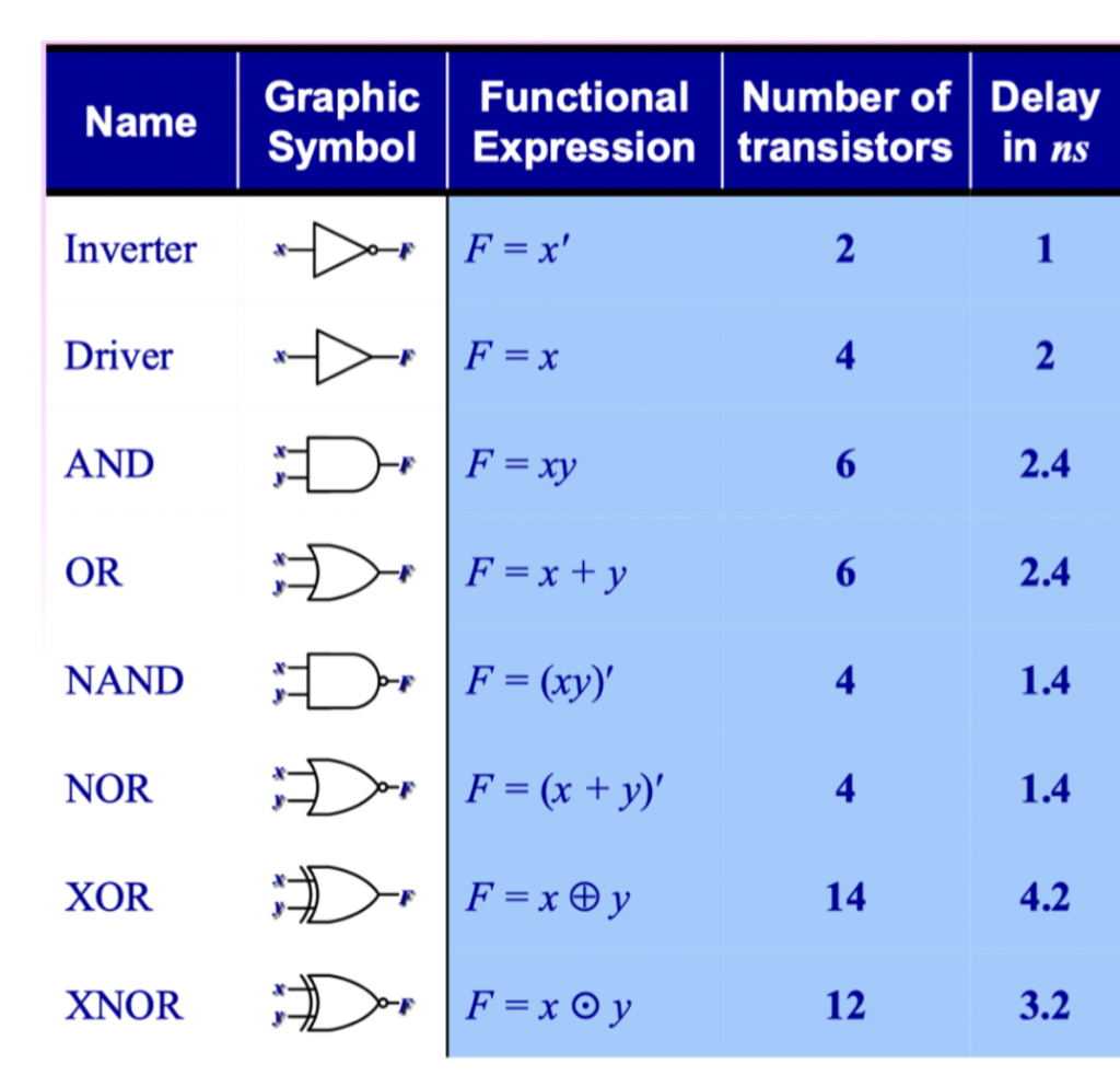
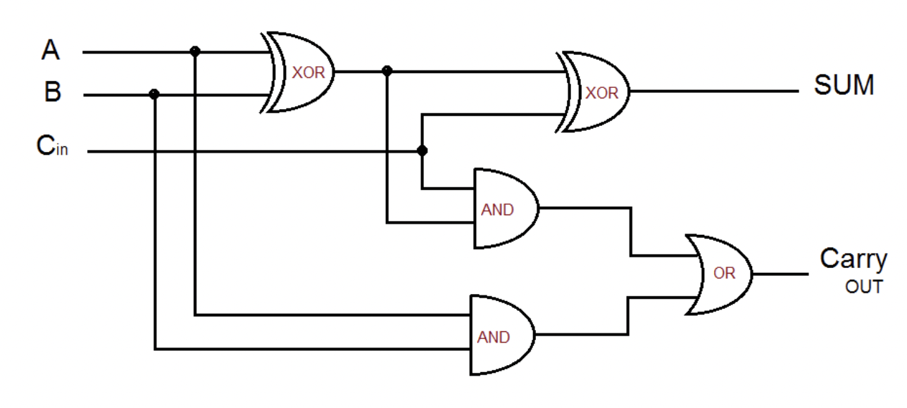
Ci+1 = ((c(xy')')'(xy)) ((t'y c)'(2'yc)(xy'd)(cyc)) Si A B XOR XOR SUM Cin AND OR Carry OUT AND Cost: transistors ns ns Delay of c; to Ci+1: Delay of c; to si: Delay of Xi,yi to Ci+1: Delay of Xi,yi to si: ns ns Name Graphic Functional Number of Delay Symbol Expression transistors Inverter F = x' 2 1 Driver F = x 4 2 AND F = xy 6 2.4 OR Du F=x + y 6 2.4 NAND F = (xy)' 4 1.4 NOR F = (x + y)' 4 1.4 XOR F = xy 14 4.2 D Da XNOR F = x Oy 12 3.2 Ci+1 = ((c(xy')')'(xy)) ((t'y c)'(2'yc)(xy'd)(cyc)) Si A B XOR XOR SUM Cin AND OR Carry OUT AND Cost: transistors ns ns Delay of c; to Ci+1: Delay of c; to si: Delay of Xi,yi to Ci+1: Delay of Xi,yi to si: ns ns Name Graphic Functional Number of Delay Symbol Expression transistors Inverter F = x' 2 1 Driver F = x 4 2 AND F = xy 6 2.4 OR Du F=x + y 6 2.4 NAND F = (xy)' 4 1.4 NOR F = (x + y)' 4 1.4 XOR F = xy 14 4.2 D Da XNOR F = x Oy 12 3.2
Step by Step Solution
There are 3 Steps involved in it

Get step-by-step solutions from verified subject matter experts