

Question: Draw the logic block diagram for a memory with 8 K words of data, where each word is 1 6 bits. The memory accesses the
Draw the logic block diagram for a memory with K words of data, where each word is bits. The memory accesses the data in chunks of one word ie for each read or write, one word of data is read out or written in respectively Show the optimum size for the memory array, the number of address anddata lines required, and any supporting logic blocks eg see Fig. in your textbook
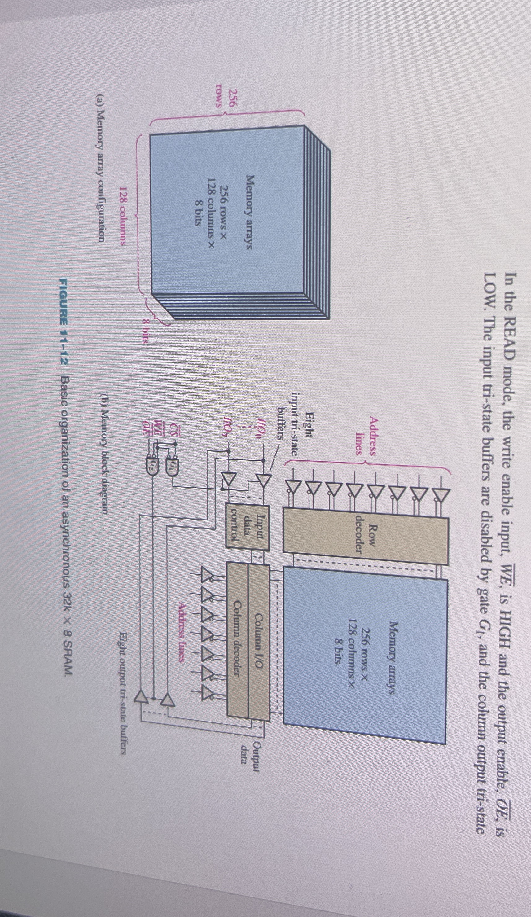
In the READ mode, the write enable input, is HIGH and the output enable, is LOW. The input tristate buffers are disabled by gate and the column output tristate
columns
Eight output tristate buffers
a Memory array configuration
b Memory block diagram
FIGURE Basic organization of an asynchronous SRAM,
Step by Step Solution
There are 3 Steps involved in it
1 Expert Approved Answer
Step: 1 Unlock

Question Has Been Solved by an Expert!
Get step-by-step solutions from verified subject matter experts
Step: 2 Unlock
Step: 3 Unlock