

Question: EET 316 DIGITAL DESIGN LAB 9 DESIGN SIMULATION OF SEQUENTIAL CIRCUITS (FUNCTIONAL VERIFICATION) Lab Summary This lab teaches Simulation (Functional Verification) using Xilinx ISE Simulator
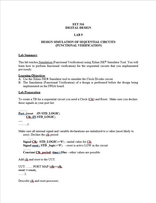
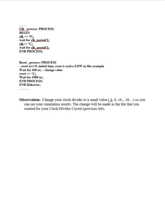
EET 316 DIGITAL DESIGN LAB 9 DESIGN SIMULATION OF SEQUENTIAL CIRCUITS (FUNCTIONAL VERIFICATION) Lab Summary This lab teaches Simulation (Functional Verification) using Xilinx ISE Simulator Tool. You will learn how to perform functional verification) for the sequential circuits that you implemented previously Learning Objectives A Use the Xilinx ISE & Simulator tool to simulate the Clock Divider circuit B. The Simulation (Functional Verification) of a design is performed before the design being implemented on the FPGA board. Lab Preparation To create a TB for a sequential circuit you need a Clock (Cik) and Reset. Make sure you declare these signals in your port list. Port (reset :IN STD_LOGIC; Cik :IN STD_LOGIC; Make sure all internal signal and variable declarations are initialized to a value (most likely to zero). Declare the clk period. Signal Cik: STD_LOGIC:='0'; -initial value for Clk Signal reset: STD_logic:="0"; --reset is active LOW in the circuit Constant Clk.period: time:=10ns --other values are possible Add clk and reset to the UUT, UUT: ...... PORT MAP (cl=ck. reset =>reset, Describe clk and reset processes. Cik process: PROCESS BEGIN clk 0: wait for clk period/2: clk 1: wait for clk period 2: END PROCESS; Reset_process: PROCESS -reset at t=0, initial time, reset is active LOW in this example Wait for 100 ns; - change value reset1!: Wait for 1000 ns; END PROCESS; END Behavior; Observation: Change your clock divider to a small value (4. 8. 10.., 20...) so you can see your simulation results. The change will be made in the file that you created for your Clock Divider Circuit (previous lab). EET 316 DIGITAL DESIGN LAB 9 DESIGN SIMULATION OF SEQUENTIAL CIRCUITS (FUNCTIONAL VERIFICATION) Lab Summary This lab teaches Simulation (Functional Verification) using Xilinx ISE Simulator Tool. You will learn how to perform functional verification) for the sequential circuits that you implemented previously Learning Objectives A Use the Xilinx ISE & Simulator tool to simulate the Clock Divider circuit B. The Simulation (Functional Verification) of a design is performed before the design being implemented on the FPGA board. Lab Preparation To create a TB for a sequential circuit you need a Clock (Cik) and Reset. Make sure you declare these signals in your port list. Port (reset :IN STD_LOGIC; Cik :IN STD_LOGIC; Make sure all internal signal and variable declarations are initialized to a value (most likely to zero). Declare the clk period. Signal Cik: STD_LOGIC:='0'; -initial value for Clk Signal reset: STD_logic:="0"; --reset is active LOW in the circuit Constant Clk.period: time:=10ns --other values are possible Add clk and reset to the UUT, UUT: ...... PORT MAP (cl=ck. reset =>reset, Describe clk and reset processes. Cik process: PROCESS BEGIN clk 0: wait for clk period/2: clk 1: wait for clk period 2: END PROCESS; Reset_process: PROCESS -reset at t=0, initial time, reset is active LOW in this example Wait for 100 ns; - change value reset1!: Wait for 1000 ns; END PROCESS; END Behavior; Observation: Change your clock divider to a small value (4. 8. 10.., 20...) so you can see your simulation results. The change will be made in the file that you created for your Clock Divider Circuit (previous lab)
Step by Step Solution
There are 3 Steps involved in it

Get step-by-step solutions from verified subject matter experts