

Question: Electronics 2 Please complete showing work and using LTspice THANK YOU ! Objective of this design project. The objectives of this design project are: (i)
Electronics 2
Please complete showing work and using LTspice
THANK YOU !
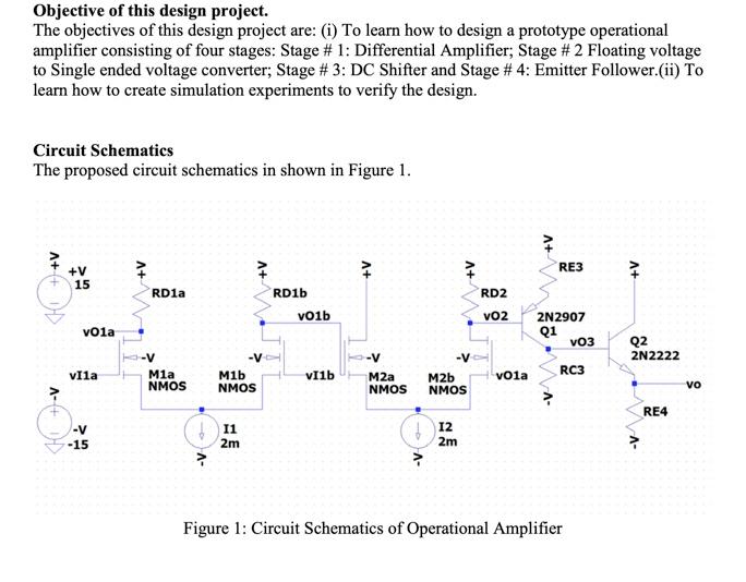
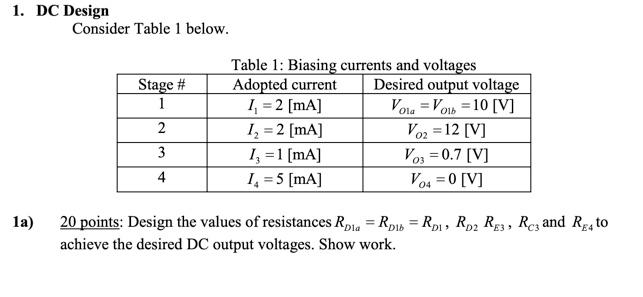
Objective of this design project. The objectives of this design project are: (i) To learn how to design a prototype operational amplifier consisting of four stages: Stage # 1: Differential Amplifier; Stage # 2 Floating voltage to Single ended voltage converter; Stage #3: DC Shifter and Stage #4: Emitter Follower.(ii) To learn how to create simulation experiments to verify the design. Circuit Schematics The proposed circuit schematics in shown in Figure 1. + +V +V 15 +V RE3 A+ RDla RD1b RD2 vo1b VO2 vola 2N2907 Q1 VO3 Q2 2N2222 vila -V Mia NMOS vilb -V 2 NMOS M1b NMOS -V M2b NMOS vola RC3 vo RE4 -V -15 11 2m 12 2m -V Figure 1: Circuit Schematics of Operational Amplifier 1. DC Design Consider Table 1 below. Table 1: Biasing currents and voltages Stage # Adopted current Desired output voltage 1 1 = 2 [mA] Vola = V016 = 10 [V] 2 1= 2 [mA] Vo2 = 12 [V] 3 13 = 1 [mA] Vo = 0.7 [V] 4 1. = 5 [mA] Vox = 0 [V] 1a) 20 points: Design the values of resistances Rpia = Rp10 = Rp, Rp2 Rg, Rc; and Reto achieve the desired DC output voltages. Show work. Objective of this design project. The objectives of this design project are: (i) To learn how to design a prototype operational amplifier consisting of four stages: Stage # 1: Differential Amplifier; Stage # 2 Floating voltage to Single ended voltage converter; Stage #3: DC Shifter and Stage #4: Emitter Follower.(ii) To learn how to create simulation experiments to verify the design. Circuit Schematics The proposed circuit schematics in shown in Figure 1. + +V +V 15 +V RE3 A+ RDla RD1b RD2 vo1b VO2 vola 2N2907 Q1 VO3 Q2 2N2222 vila -V Mia NMOS vilb -V 2 NMOS M1b NMOS -V M2b NMOS vola RC3 vo RE4 -V -15 11 2m 12 2m -V Figure 1: Circuit Schematics of Operational Amplifier 1. DC Design Consider Table 1 below. Table 1: Biasing currents and voltages Stage # Adopted current Desired output voltage 1 1 = 2 [mA] Vola = V016 = 10 [V] 2 1= 2 [mA] Vo2 = 12 [V] 3 13 = 1 [mA] Vo = 0.7 [V] 4 1. = 5 [mA] Vox = 0 [V] 1a) 20 points: Design the values of resistances Rpia = Rp10 = Rp, Rp2 Rg, Rc; and Reto achieve the desired DC output voltages. Show work
Step by Step Solution
There are 3 Steps involved in it

Get step-by-step solutions from verified subject matter experts