Question: F a . To have a lower switching threshold voltage for a CMOS inverter, it is required to make the PMOS larger than the NMOS.
F
a To have a lower switching threshold voltage for a CMOS inverter, it is required to make the PMOS larger than the NMOS.
b The diffusion capacitance is a function in the operating voltage VGS & VDS of the MOS transistor.
F
c In a CMOS inverter, increasing the transistor widths N and P causes the short circuit power to decrease
F
d In a CMOS inverter, increasing the output load capacitance CL may cause the static power dissipation to increase
F
e Decreasing the transistor threshold voltage, causes the short circuit power dissipation to
f There is a maximum value for the output load capacitance of a CMOS inverter that should not be exceeded.
g Short circuit power can be neglected in short channel technologies
h The delay of a CMOS inverter is affected by the size of the gates it is driving but not the size of the gates it is driven by
i In short channel MOSFET transistors that are deployed in digital circuits, the likelihood that pinch off saturation takes place is higher than being in velocity saturation.
j From an architecture point of view, increasing the operating frequency always leads to an increase in the total power consumption
k Body effect does not affect PMOS transistors
Rise and fall times describe differences in timing between two waveforms
m The maximum number of inputs connected to gate is called fan out
n We size PMOS double NMOS in the unit inverter because PMOS suffers more from velocity saturation
: Short circuit power dissipation in a CMOS inverter depends largely on the slope of the output waveform
p Using a lower permittivity dielectric in MOSFETs leads to reduced capacitance and higher resistanceuestion marks
pts for eadi give ging reasons either way
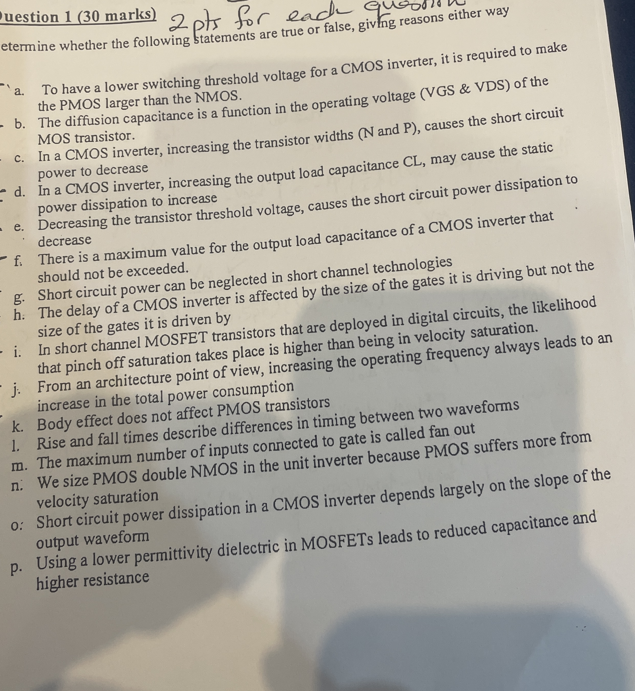
etermine whether the following statements are true or false, giving reasons
a To have a lower switching threshold voltage for a CMOS inverter, it is required to make the PMOS larger than the NMOS.
b The diffusion capacitance is a function in the operating voltage VGS & VDS of the MOS transistor.
c In a CMOS inverter, increasing the transistor widths N and P causes the short circuit power to decrease
d In a CMOS inverter, increasing the output load capacitance CL may cause the static power dissipation to increase
e Decreasing the transistor threshold voltage, causes the short circuit power dissipation to decrease
f There is a maximum value for the output load capacitance of a CMOS inverter that should not be exceeded.
g Short circuit power can be neglected in short channel technologies
h The delay of a CMOS inverter is affected by the size of the gates it is driving but not the size of the gates it is driven by
i In short channel MOSFET transistors that are deployed in digital circuits, the likelihood that pinch off saturation takes place is higher than being in velocity saturation.
j From an architecture point of view, increasing the operating frequency always leads to an increase in the total power consumption
k Body effect does not affect PMOS transistors
Rise and fall times describe differences in timing between two waveforms
m The maximum number of inputs connected to gate is called fan out
n We size PMOS double NMOS in the unit inverter because PMOS suffers more from velocity saturation
o: Short circuit power dissipation in a CMOS inverter depends largely on the slope of the output waveform
p Using a lower permittivity dielectric in MOSFETs leads to reduced capacitance and higher resistance

Step by Step Solution
There are 3 Steps involved in it
1 Expert Approved Answer
Step: 1 Unlock


Question Has Been Solved by an Expert!
Get step-by-step solutions from verified subject matter experts
Step: 2 Unlock
Step: 3 Unlock


