

Question: Hello, this is for Digital Logic With VHDL. I have a lab that has two parts, I am to implement a 4-to-1 multiplexer and a
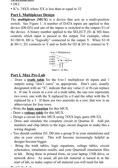
. DE2 IC's: 74XX where XX is less than or equal to 32 The multiplexer (MUX) is a device that acts as a multi-position switch. See Figure 1. A number of DATA inputs are applied to this device (D0-D3) and one of the inputs is switched to the output (Y) of the device. A binary number applied to the SELECT (S1 & SO) lines controls which input is passed to the output. For example, when si-s0-0. Do is logically" connected to the output Y. When Si-0 & S0-1, DI connects to Y and so forth for D2 & D3 to connect to Y 4-to-1 Multiplexer DI Figure 1. 4:1 Mu . Draw a truth table for the 4-to-1 multiplexer (6 inputs and 1 output) using "don't cares" as appropriate. Don't care, usually designated with an X", indicate that any value (1 or 0) can replace it. If one X exists in a row of a truth table, the one row represents two rows; one with the X replaced by a 0 and the other with the X replaced by a 1. If there are two asterisks in a row, that row is an abbreviation for four rows. 2. Write the logic equation for this MUX. . Draw a yoltage table for this MUX. 4. Design a cicuit for this MUX using 74XX logic gates (00-32). s. Draw and simulate the complete circuit in Quarts Add pin numbers and chip labels to the logic circuit diagram to make this a wiring diagram. into a group D in your simulations and 6. You Should combine DS.D0 also in your circuit. This will become increasingly helpful as designs become bigger 7. Bring the truth tables, logic equations, voltage tables, circuit schematics, simulation results, and your QuartusII simulation files to lab. Bring these in printed form, on your laptop, USB drive, or network drive. As usual, all pre-lab material is turned in at the start of lab, so make copies of all material you will need for lab
Step by Step Solution
There are 3 Steps involved in it

Get step-by-step solutions from verified subject matter experts