

Question: Homework 3 Part 2 Instructions * * * Need K - Maps and Truth Tables when needed. Need the Digital Works implementation as well *
Homework Part Instructions
Need KMaps and Truth Tables when needed. Need the Digital Works implementation as well
In this part, you are asked to design a bit ALU in Digital Works. You may break down the design into the following stepsblocks Make sure to thoroughly test every block before moving to the next step. Testing and thorough understanding of each individual macro will be evaluated during check off with the instructor. Here are more details about each block:
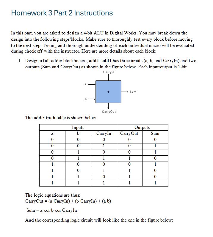
Design a full adder blockmacro addl. addl has three inputs a b and CarryIn and two outputs Sum and CarryOut as shown in the figure below. Each inputoutput is bit.
The adder truth table is shown below:
The logic equations are thus:
CarryOut mathrmacdot CarryIn mathrmbcdot CarryIn mathrmacdot mathrmb
Sum mathrma xor b xor CarryIn
And the corresponding logic circuit will look like the one in the figure below:
For a refresher on how to extract the logic equation and circuits, check appendix in the
zybooks textbook.
Don't forget to thoroughly test the individual macro before moving to the next step.
Design a multiplexer macro, mux mux has two data inputs in and in and one
data output out Each inputoutput is bit. The multiplexer has one select line sel that
controls which input is passed to the output as shown below:
You will need to use truth table and kmap to come up with the logic equation for the
multiplexer block, and then map the logic equation to the respective logic circuit as
shown for the full adder above and as you did in CS
Don't forget to thoroughly test the individual macro before moving to the next step.
Design a multiplexer macro, mux mux has four data inputs in in in and
in and one data output out Each inputoutput is bit. The multiplexer has a bit
selection line sell and sel that controls which input is passed to the output. Hint: you
may use of the mux macros from step to build this multiplexer as shown below:
Design bit ALU macro, alu using the two multiplexer macros and the full adder
macro from the previous steps. The ALU has three data inputs ab and less four
control signals Binvert CarryIn, Operation and Operation and one data output
Result as shown in the following figure. The ALU supports logical and, logical or add,
subtract, and set if less than operations as explained in class.
Don't forget to thoroughly test the bit ALU before moving to the next step.
Note: you may need to create another macro alulextra that is a copy of alul but
has an additional output called Set which is the adder output. This will be used as
ALU in the next step to support the sit functionality.
Design a bit ALU using the alul macro from step and aluextra The bit ALU
has two data inputs a and b and one data output Resultbits each you may call
them aaa and a and so on The ALU also has four control signals Binvert
CarryIn, Operation and Operation as explained in the lecture and depicted in the
picture below. Note that the ALU picture from the slides has alul but, in this
homework, you only need to have alul macros and alulextra macro. The less input
for ALUO is connected to Set output of ALU which is the adder output for the most
significant alu ALU The less data input is for the remaining alus ALU ALU
and ALU You may ignore the overflow detection output shown below.
Step by Step Solution
There are 3 Steps involved in it
1 Expert Approved Answer
Step: 1 Unlock

Question Has Been Solved by an Expert!
Get step-by-step solutions from verified subject matter experts
Step: 2 Unlock
Step: 3 Unlock