

Question: ------------------------------------------------------------------------------------------------------------------------------------------------------------------------------------------------------------------------------------------------------------------- I already have the source code, but I'm not entirely sure how to do the test bench. I'm doing this in Xilinx ISE Design
-------------------------------------------------------------------------------------------------------------------------------------------------------------------------------------------------------------------------------------------------------------------
I already have the source code, but I'm not entirely sure how to do the test bench. I'm doing this in Xilinx ISE Design Tools, just for clarification.
Heres the source code:
module register (input clk,
input reset,
input Reg_Write_Enable,
input [2:0] Reg_Write_Dst,
input [15:0] Reg_Write_Data,
input [2:0] Reg_Read_src_1,
output [15:0] Reg_Read_data_1,
input [2:0] Reg_Read_src_2,
output [15:0] Reg_Read_data_2);
reg [15:0] regfile [0:7];
assign rdDataA = regfile[Reg_Read_src_1];
assign rdDataB = regfile[Reg_Read_src_2];
always @(posedge clk) begin
if (reset) begin
regfile[0]
regfile[1]
regfile[2]
regfile[3]
regfile[4]
regfile[5]
regfile[6]
regfile[7]
end else begin
if (Reg_Write_Enable) regfile[Reg_Write_Dst]
end // else: !if(reset)
end
endmodule
So, now I just need to figure out this testbench. If anyone could help me out that would be fantastic! Thank you :)!
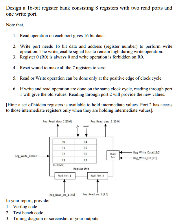
Design a 16-bit register bank consisting 8 registers with two read ports and one write port. Note that, 1. Read operation on each port gives 16 bit data. 2. Write port needs 16 bit data and address (register number) to perform write operation. The write enable signal has to remain high during write operation. 3. Register 0 (RO) is always 0 and write operation is forbidden on RO. 4. Reset would to make all the 7 registers to zero. 5. Read or Write operation can be done only at the positive edge of clock cycle. 6. If write and read operation are done on the same clock cycle, reading through port l will give the old values. Reading through port 2 will provide the new values. [Hint: a set of hidden registers is available to hold intermediate values. Port 2 has access to those intermediate registers only when they are holding intermediate values] Reg Read data 21150 Reg Read data 1[15:0] dk reset RO R4 write Reg Write. Data[15:0] Reg Write Enable- Reg Write. Dst 12:0 R3 R7 RO-0(fixed) Register Unit Read Port 1 Read Port 2 Reg Read src 112:0] Reg Read src 202:01 In your report, provide: 1. Verilog code 2. Test bench code 3. Timing diagram or screenshot of your outputs
Step by Step Solution
There are 3 Steps involved in it

Get step-by-step solutions from verified subject matter experts