

Question: I am having a hard time understanding how the instructions work. Here is just a couple of the instructions that need to be dealt with.
I am having a hard time understanding how the instructions work. Here is just a couple of the instructions that need to be dealt with. Can anyone explain to me how to find the solution to this? Here are just a couple of instructions that I would like help understanding. Any help would be greatly appreciated.
MAR:= PC;RD
MAR:=PC; MBR:=AC; WR
IR:= MBR
TIR:= IR; GOTO 25
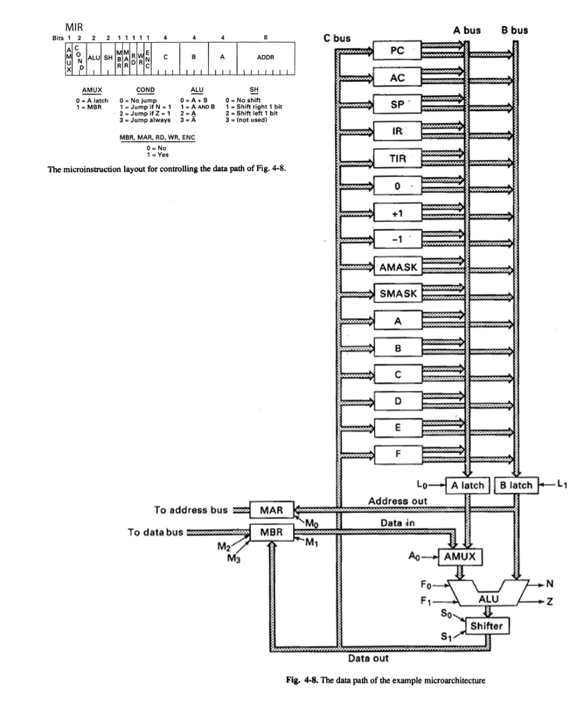
MIR A bus B bus C bus PC D?R AC SP IR TIR ALU COND 0 A latch 0 No jump SH 0 No shift AMUX 0 A+B 1 MBR Jump if N-1 1- A AND B 1 2-Jump if Z = 1 2 3 Jump always 3 Shift right 1 bit 2 Shift left 1 bit 3-(not used) MBR, MAR, RD, WR, ENC 0 No 1 Yes The microinstruction layout for controlling the data path of Fig. 4-8 AMASK SMASK A latchB latch Address out To address bus MAR Data in To data bus MBR ALU Shifter Data out Fig. 4-8. The data path of the example microarchitecture
Step by Step Solution
There are 3 Steps involved in it

Get step-by-step solutions from verified subject matter experts