

Question: I can't understand what is this circuit's operation. Please explain to me in detail this circuit is used for FPGA and inverter following the input
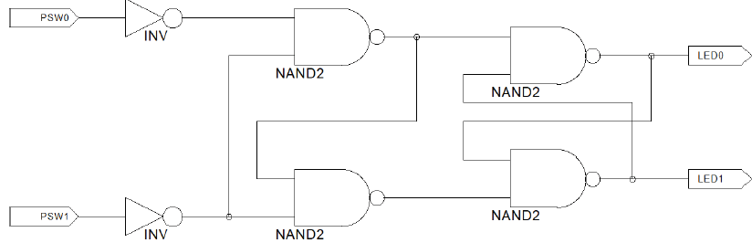
I can't understand what is this circuit's operation. Please explain to me in detail
this circuit is used for FPGA and inverter following the input data is just for easy interpretation considering the KIT
It is not a general D latch. see the wire arrangement carefully. thanks :D
PSWO INV LEDO NAND2 NAND2 LED1 PSW1 NAND2 INV NAND2 PSWO INV LEDO NAND2 NAND2 LED1 PSW1 NAND2 INV NAND2
Step by Step Solution
There are 3 Steps involved in it
1 Expert Approved Answer
Step: 1 Unlock

Question Has Been Solved by an Expert!
Get step-by-step solutions from verified subject matter experts
Step: 2 Unlock
Step: 3 Unlock