

Question: i need step by step pleasee o Problem Situation Using universal gate NAND gates only, design a logic circuit that controls an LRT coach door


i need step by step pleasee
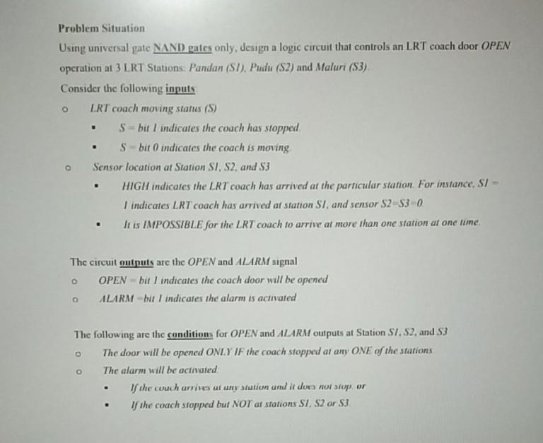
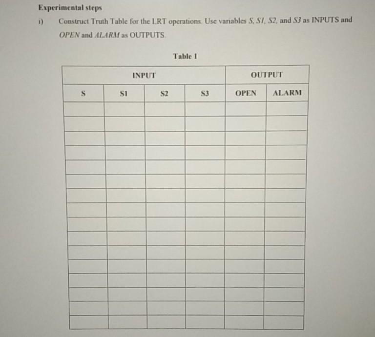
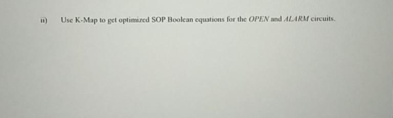
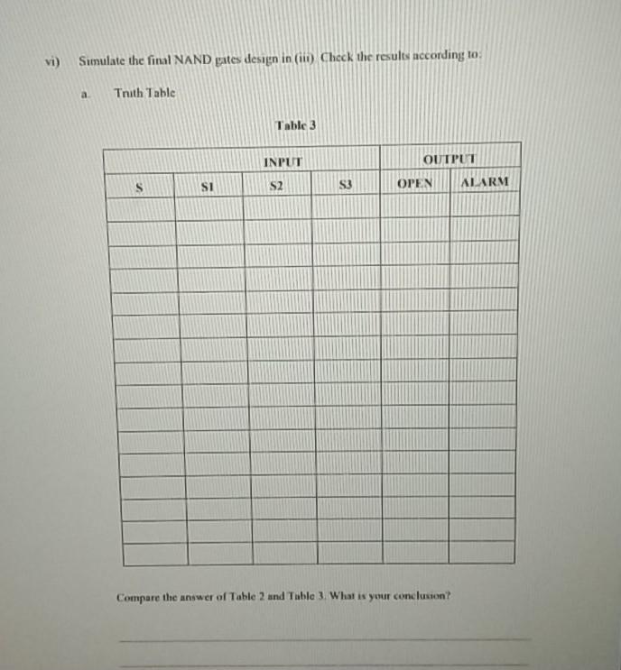
o Problem Situation Using universal gate NAND gates only, design a logic circuit that controls an LRT coach door OPEN operation at 3 LRT Stations. Pandan (SI). Pudu (S2) and Maluri (53) Consider the following inputs LRT coach moving status (S) S = bit I indicates the coach has stopped Sbito indicates the coach is moving Sensor location at Station SI, S2. and S3 HIGH indicates the LRT coach has arrived at the particular station. For instance, SI I indicates LRT coach has arrived at station SI, and sensor S2 S30 It is IMPOSSIBLE for the LRT coach to arrive at more than one station at one time The circuit outputs are the OPEN and ALARM signal OPEN bit l indicates the coach door will be opened ALARM but I indicates the alarm is activated O O The following are the conditions for OPEN and ALARM outputs at Station ST. S. and S3 The door will be opened ONLY IF the coach stopped at any ONE of the stations The alarm will be activated If the couch arrives at any atution and it does not stup or If the coach stopped but NOT at stations S1, S2 or $3. 0 . Experimental steps Construct Truth Table for the LRT operations. Use variables S, SI, S2, and S3 as INPUTS and OPEN and ALARM as OUTPUTS Table 1 INPUT OUTPUT S SI S2 S3 OPEN ALARM 11) Use K-Map to get optimized SOP Boolcan equations for the OPEN and ALARM circuits in From equations in (i), draw your final OPEN and ALARM circuits iv) Simulate the circuit design in (ii). Check the results according to Truth Table Table 2 INPUT OUTPUT S SI S2 S3 OPEN ALARM Compare the answer of Table 2 and Table 1. What is your conclusion? b. Timing Diagram Show some analysis values: Use dual symbol to convert, AND OR circuit to NAND gates only. Draw the final circuit using Deeds Simulator vi) Sumulate the final NAND gates design in (1) Check the results according to a Tnith Table Table 3 INPUT OUTPUT SI S2 S3 OPEN ALARM Compare the answer of Table 2 and Table 3. What is your conclusion? b Timing Diagram Show some analysis values
Step by Step Solution
There are 3 Steps involved in it

Get step-by-step solutions from verified subject matter experts