

Question: I only need the second question. Thank you. 8. (25) (Bulk Microfabrication, MEMS capacitor design) The electronic connection routing of a capacitive accelerometer is illustrated
I only need the second question. Thank you.
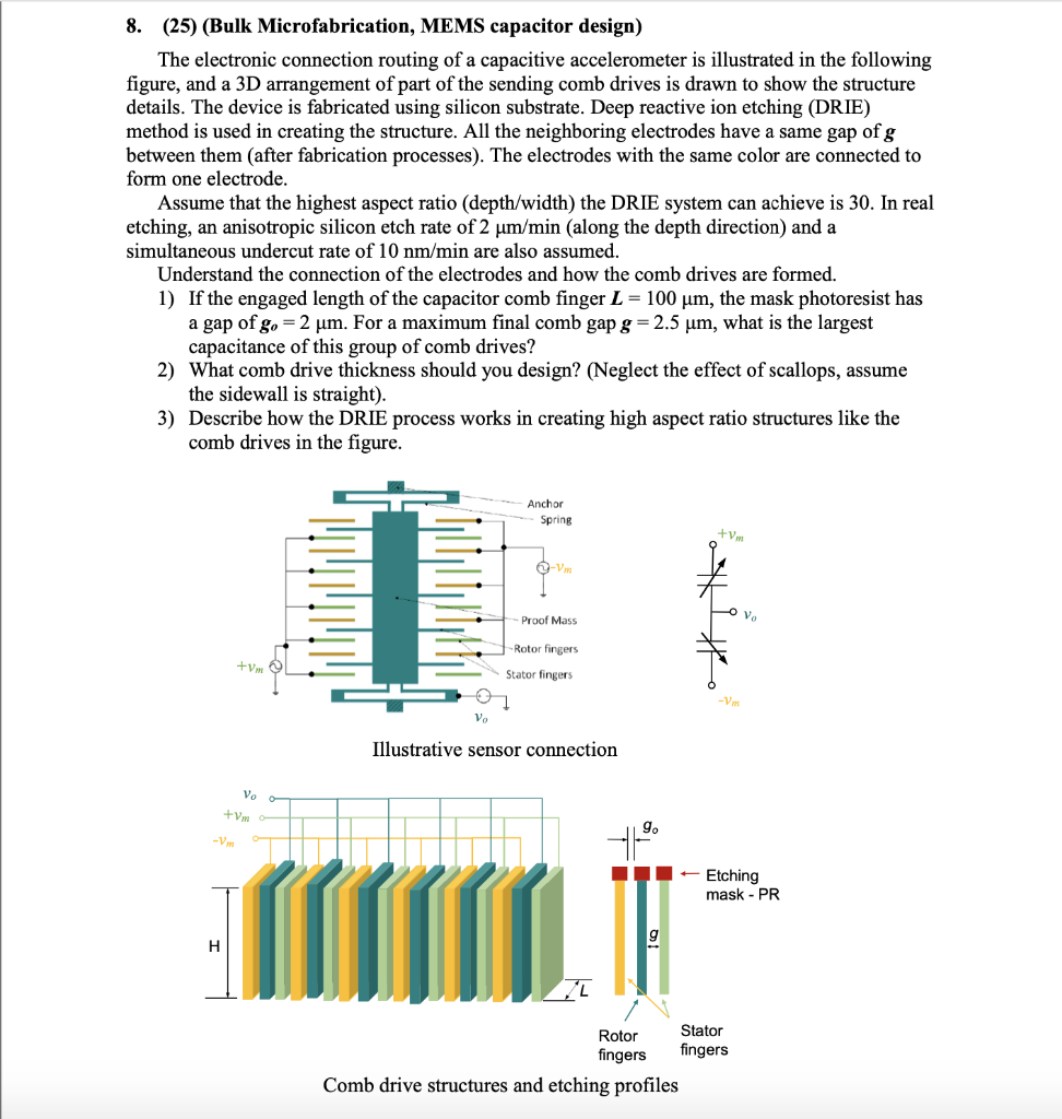
8. (25) (Bulk Microfabrication, MEMS capacitor design) The electronic connection routing of a capacitive accelerometer is illustrated in the following figure, and a 3D arrangement of part of the sending comb drives is drawn to show the structure details. The device is fabricated using silicon substrate. Deep reactive ion etching (DRIE) method is used in creating the structure. All the neighboring electrodes have a same gap of g between them (after fabrication processes). The electrodes with the same color are connected to form one electrode. Assume that the highest aspect ratio (depth/width) the DRIE system can achieve is 30. In real etching, an anisotropic silicon etch rate of 2 um/min (along the depth direction) and a simultaneous undercut rate of 10 nm/min are also assumed. Understand the connection of the electrodes and how the comb drives are formed. 1) If the engaged length of the capacitor comb finger L = 100 um, the mask photoresist has a gap of go = 2 um. For a maximum final comb gap g=2.5 um, what is the largest capacitance of this group of comb drives? 2) What comb drive thickness should you design? (Neglect the effect of scallops, assume the sidewall is straight). 3) Describe how the DRIE process works in creating high aspect ratio structures like the comb drives in the figure. Anchor Spring +V. Proof Mass -Rotor fingers + Stator fingers V. Illustrative sensor connection Vo +Vw 9. II-Etching mask - PR g H Rotor Stator fingers fingers Comb drive structures and etching profiles 8. (25) (Bulk Microfabrication, MEMS capacitor design) The electronic connection routing of a capacitive accelerometer is illustrated in the following figure, and a 3D arrangement of part of the sending comb drives is drawn to show the structure details. The device is fabricated using silicon substrate. Deep reactive ion etching (DRIE) method is used in creating the structure. All the neighboring electrodes have a same gap of g between them (after fabrication processes). The electrodes with the same color are connected to form one electrode. Assume that the highest aspect ratio (depth/width) the DRIE system can achieve is 30. In real etching, an anisotropic silicon etch rate of 2 um/min (along the depth direction) and a simultaneous undercut rate of 10 nm/min are also assumed. Understand the connection of the electrodes and how the comb drives are formed. 1) If the engaged length of the capacitor comb finger L = 100 um, the mask photoresist has a gap of go = 2 um. For a maximum final comb gap g=2.5 um, what is the largest capacitance of this group of comb drives? 2) What comb drive thickness should you design? (Neglect the effect of scallops, assume the sidewall is straight). 3) Describe how the DRIE process works in creating high aspect ratio structures like the comb drives in the figure. Anchor Spring +V. Proof Mass -Rotor fingers + Stator fingers V. Illustrative sensor connection Vo +Vw 9. II-Etching mask - PR g H Rotor Stator fingers fingers Comb drive structures and etching profiles
Step by Step Solution
There are 3 Steps involved in it

Get step-by-step solutions from verified subject matter experts