

Question: Implement the following circuit using the modules that you have implemented in PART 1 . For FFs , you should use one single synchronous reset.
Implement the following circuit using the modules that you have implemented in PART For FFs you should use one single synchronous reset. You have input ports, ie X Y Z S S and one output port T For this part only: The TA will check your schematic and code instead of the testbench simulation. To access the schematic in Vivado, first click on Open Elaborated Design You should double check that your schematic matches the circuit below.
Add a synchronous reset as an input to DFF
Make a new module and reuse your old code to add an asynchronous reset
to DFF
Implement a positive edge triggered TFF using the DFF without the reset.
Add a synchronous reset as an input to TFF you can use the DFF from step
Make a new module and reuse your old code to add an asynchronous reset
to TFF you can use the DFF from step
Use the DFF and now construct a JKFF
a Use the DFF without reset to build a JKFF without reset.
b Use the DFF with synchronous reset to build a JKFF with
synchronous reset.
c Use the DFF with asynchronous reset to build a JKFF with
asynchronous reset.
Instantiate two versions of JKFFs with synchronous and asynchronous
resets in your top module.
a Two JKFF modules will share the same inputs J K reset, and clock.
b The final outputs of top module will be the output Qsync from JKFF
with synchronous reset and Qasync from JKFF with asynchronous
reset.
c Qsync and Qasync should be the outputs.
d Your testbench must test at least one case where Qsync and
Qasync are different.
For each of the steps, build a test bench that shows your modules work. There are
few inputs, so test them exhaustively.
Part B:
Use the DFF and the clock divider provided to you and divide the system clock by
to create a x slower clock and use it as the clock of the DFF Run a testbench and
verify the DFF changes output at posedge of the slower clock.
CLOCK DIVIDER
The reason you want that clock to be slow is that when you move the switches in
case you implement the design on FPGA you can observe the DFF output. We
provided you a clock divider Verilog file cl kdivider.v You need to
understand the implementation of this file and make changes to satisfy required
clock frequency.
PART
Part A:
In this part, you will implement three different types of FFs with two different reset
types. You must show your results using simulation. You must use behavioral
Verilog for the FFs
Steps:
Build a positive edge triggered DFFWe did this step for you as an example.
Please use the given dffv and dfftbv files
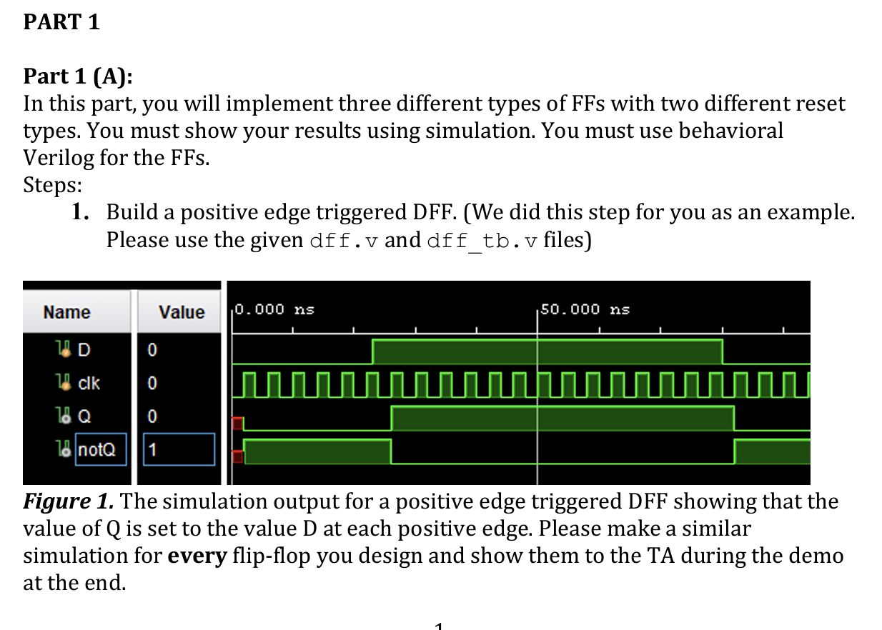
Figure The simulation output for a positive edge triggered DFF showing that the
value of Q is set to the value D at each positive edge. Please make a similar
simulation for every flipflop you design and show them to the TA during the demo
at the end. for dff timescale ns ps
Company:
Engineer:
Create Date: :: AM
Design Name:
Module Name: dff
Project Name:
Target Devices:
Tool Versions:
Description:
Dependencies:
Revision:
Revision File Created
Additional Comments:
module dff
input D
input clk
output reg Q
output notQ
;
initial Q ;
assign notQ ~Q;
always @posedge clk begin
Q D;
end
endmodule
Step by Step Solution
There are 3 Steps involved in it
1 Expert Approved Answer
Step: 1 Unlock

Question Has Been Solved by an Expert!
Get step-by-step solutions from verified subject matter experts
Step: 2 Unlock
Step: 3 Unlock