

Question: LOGIC DESIGN PLEASE ANSWER WITH ALL STEPS. ANY SPAM OR COPIED WRONG ANSWER WILL BE MARKED SPAM AND WILL BE REPORTED TO CHEGG AND YOUR
LOGIC DESIGN
PLEASE ANSWER WITH ALL STEPS. ANY SPAM OR COPIED WRONG ANSWER WILL BE MARKED SPAM AND WILL BE REPORTED TO CHEGG AND YOUR ACCOUNT MAY BE DEACTIVATED BY CHEGG. IM UPLOADING THE SAME QUESTION FOR THE 5th TIME, SO I WILL MAKE SURE YOUR ACCOUNT IS DEACTIVATED IF YOU SENd ME A SPAM OR INCOMPLETE ANSWER! I HAVE COMPLAINED TO CHEGG ABOUT THE OTHER RESPONSES I GOT.
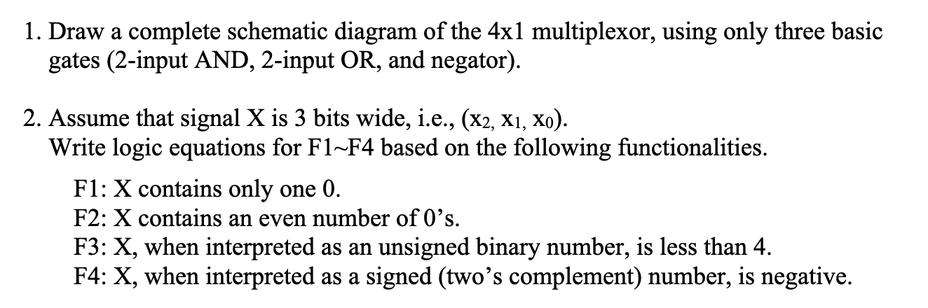
1. Draw a complete schematic diagram of the 4x1 multiplexor, using only three basic gates (2-input AND, 2-input OR, and negator). 2. Assume that signal X is 3 bits wide, i.e., (X2, X1, Xo). Write logic equations for F1-F4 based on the following functionalities. F1: X contains only one 0. F2: X contains an even number of O's. F3: X, when interpreted as an unsigned binary number, is less than 4. F4: X, when interpreted as a signed (two's complement) number, is negative
Step by Step Solution
There are 3 Steps involved in it
To solve these problems lets break them down into parts 1 Schematic Diagram of a 4x1 Multiplexer A 4... View full answer

Get step-by-step solutions from verified subject matter experts