

Question: Logic Gate Design using multiplexers for full adder functionality I am currently learning Verilog and how to use full adders. I am currently facing an
Logic Gate Design using multiplexers for full adder functionality
I am currently learning Verilog and how to use full adders. I am currently facing an issue with how to build full adders using purely multiplexers. I was able to create one Full adder through the use of the Geeks for Geeks example below:
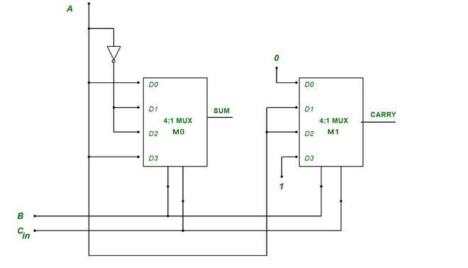
However, I am wanting to create multiple full adders so I that I can create about n ripple carry adders. Say I want to connect one full adder to another; how would I go about the connection? I am currently having trouble understanding what comes next and how to be able to calculate for the next inputs for the multiplexers for the second full adder when connected. My main confusion stems from having a different carry out and a different Cin in the full adder truth table. The main objective is to create a number of Full adders, connect these Full adders together to create a ripple carry adder, but you must implement each full adder with two 4-1 muxes, one inverter, and 0's and 1's as needed. I have been able to complete one Full adder as so but I am having trouble connecting the "converted" full adder to other full adders.
A 0 DO DO D1 SUM D1 CARRY 4:1 MUX MO 4:1 MUX M1 D2 D2 D3 D3 B Cin
Step by Step Solution
There are 3 Steps involved in it

Get step-by-step solutions from verified subject matter experts