

Question: materials science, nanotechnology only need B A 1m1m feature needs to be written on PMMA coated Si substrate using scanning probe lithography that employs an
materials science, nanotechnology
only need B
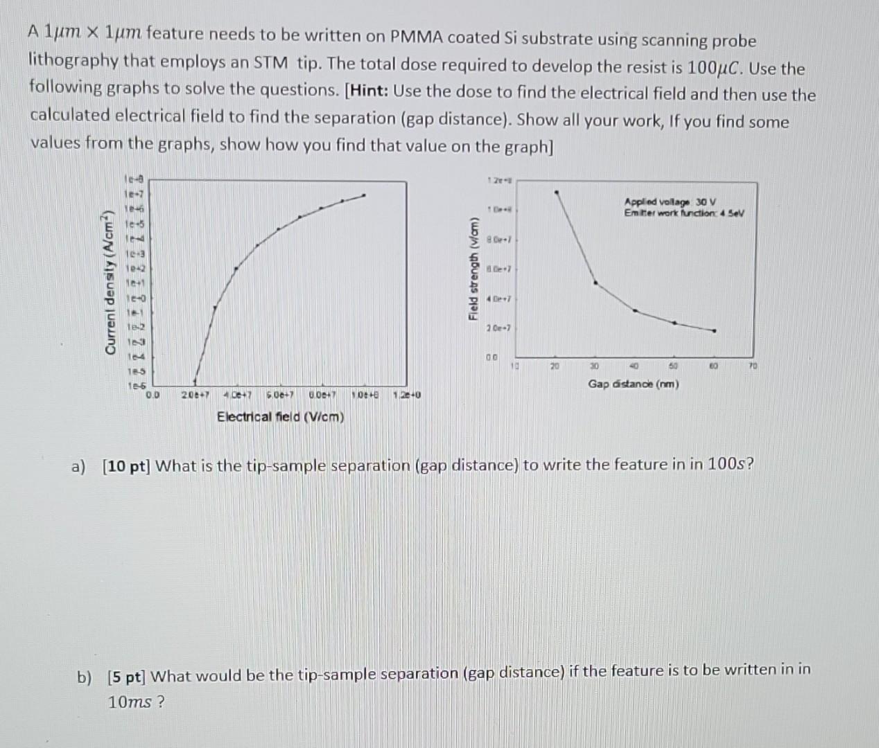
A 1m1m feature needs to be written on PMMA coated Si substrate using scanning probe lithography that employs an STM tip. The total dose required to develop the resist is 100C. Use the following graphs to solve the questions. [Hint: Use the dose to find the electrical field and then use the calculated electrical field to find the separation (gap distance). Show all your work, If you find some values from the graphs, show how you find that value on the graph] a) [10 pt] What is the tip-sample separation (gap distance) to write the feature in in 100 s? b) [ 5pt] What would be the tip-sample separation (gap distance) if the feature is to be written in in 10ms
Step by Step Solution
There are 3 Steps involved in it

Get step-by-step solutions from verified subject matter experts