

Question: 1. A) Identify the following transistors, indicating name, n-channel, p-channel, depletion, enhancement types. OD 9D 9D D O SS i) 1 B) i) Mark
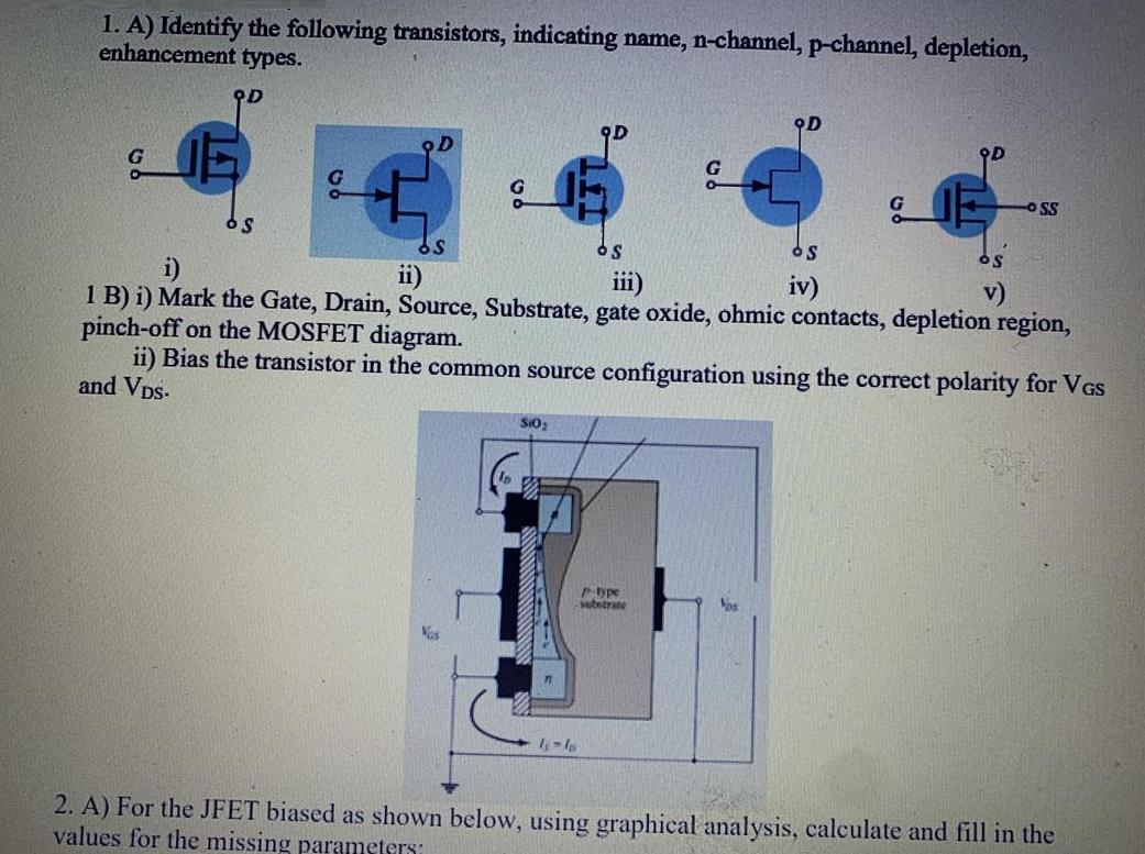
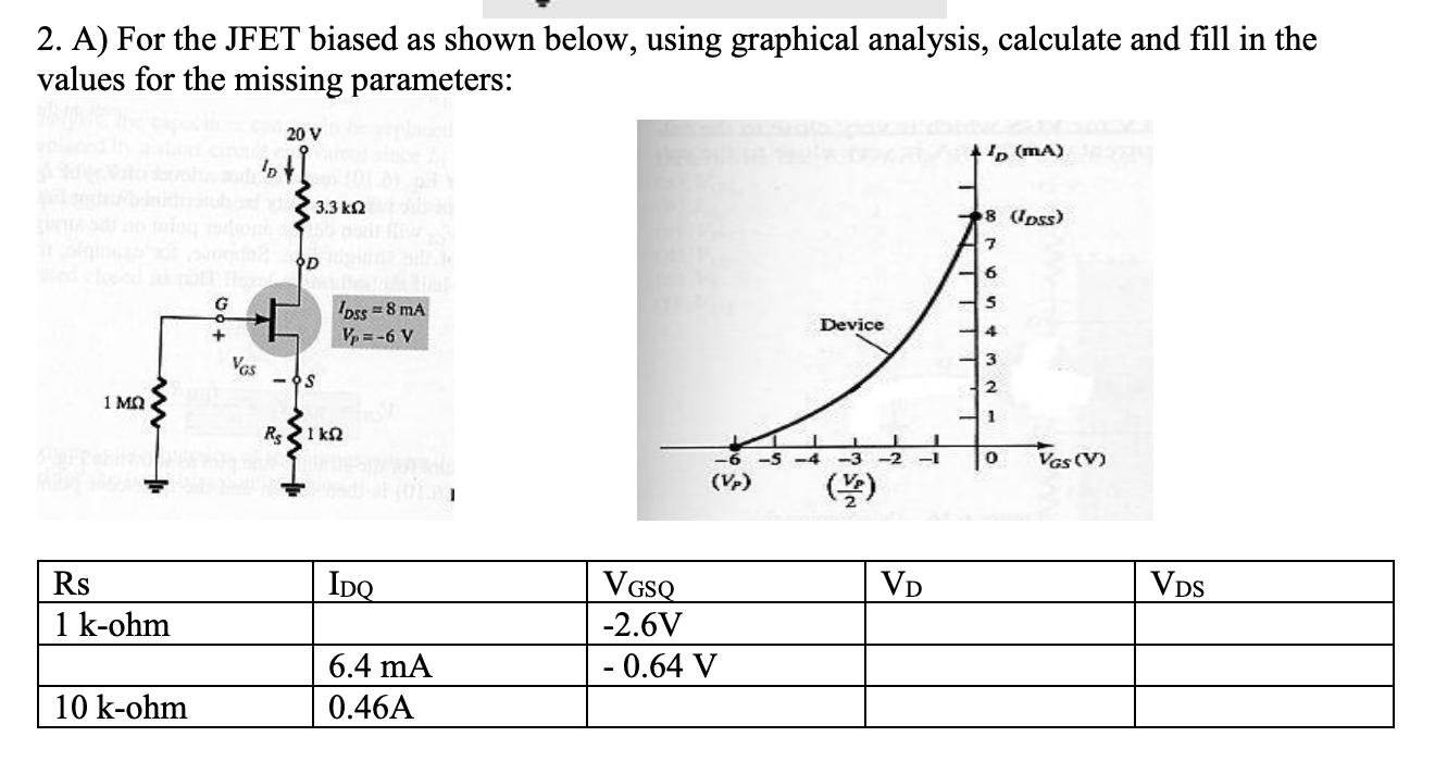
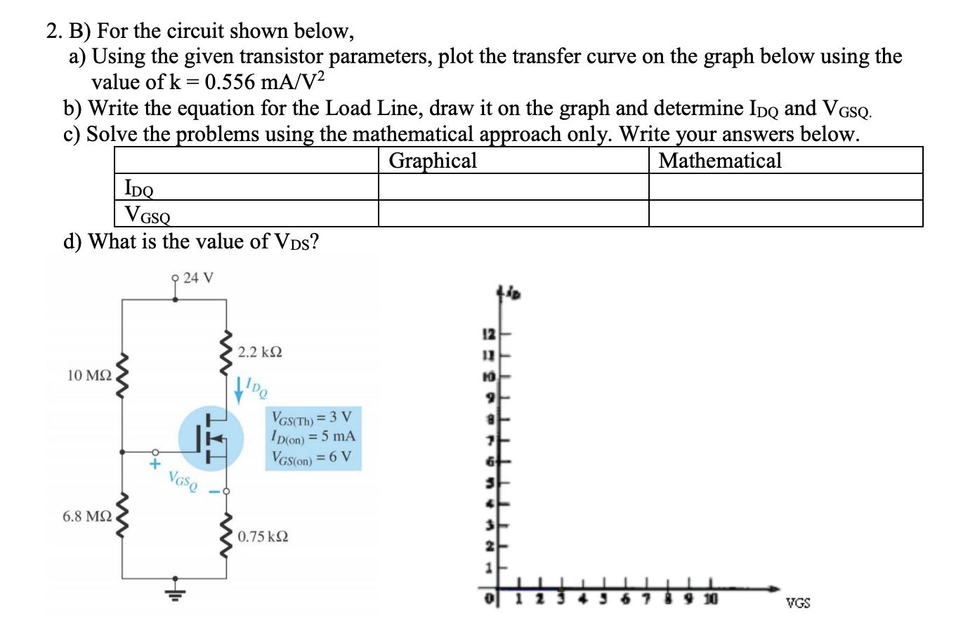
1. A) Identify the following transistors, indicating name, n-channel, p-channel, depletion, enhancement types. OD 9D 9D D O SS i) 1 B) i) Mark the Gate, Drain, Source, Substrate, gate oxide, ohmic contacts, depletion region, pinch-off on the MOSFET diagram. ii) Bias the transistor in the common source configuration using the correct polarity for VGS and VDs. ii) iii) iv) v) SIO: bpe sebstrate 2. A) For the JFET biased as shown below, using graphical analysis, calculate and fill in the values for the missing parameters: 2. A) For the JFET biased as shown below, using graphical analysis, calculate and fill in the values for the missing parameters: 20 V ', (mA) 3.3 k2 8 Upss) OD 6 Ipss = 8 mA V, = -6 V Device 4 Vas - Os 1 MO 1 Rs1 k2 -3 -2 -1 Vas (V) () (V) Rs IDQ VGSQ VD VDs 1 k-ohm -2.6V 6.4 mA - 0.64 V 10 k-ohm 0.46A 2. B) For the circuit shown below, a) Using the given transistor parameters, plot the transfer curve on the graph below using the value of k = 0.556 mA/V2 b) Write the equation for the Load Line, draw it on the graph and determine IpQ and VGSQ. c) Solve the problems using the mathematical approach only. Write your answers below. Graphical Mathematical IDQ VGSQ d) What is the value of VDs? 9 24 V 12 2.2 k2 10 . 10 VGS(Th) = 3 V IDon) = 5 mA VGS(on) = 6 V 6.8 . 0.75 k2 9:10 VGS
Step by Step Solution
3.44 Rating (154 Votes )
There are 3 Steps involved in it

Get step-by-step solutions from verified subject matter experts