

Question: P3 P2 P4 (a) Circuit Clock (b) Graphical symbol Figure 5.11 A positive-edge-triggered D ip flop. This circuit behaves as a positive-edge-triggered D flip-flop. A
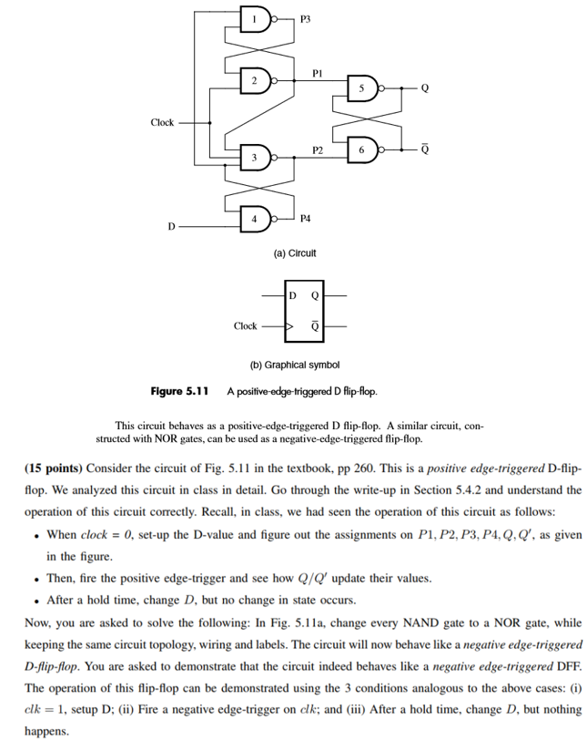
P3 P2 P4 (a) Circuit Clock (b) Graphical symbol Figure 5.11 A positive-edge-triggered D ip flop. This circuit behaves as a positive-edge-triggered D flip-flop. A similar circuit, con- structed with NOR gates, can be used as a negative-edge-triggered flip-flop. (15 points) Consider the circuit of Fig. 5.11 in the textbook, pp 260. This is a positive edge-triggered D-flip- flop. We analyzed this circuit in class in detail. Go through the write-up in Section 5.4.2 and understand the operation of this circuit correctly. Recall, in class, we had seen the operation of this circuit as follows: When clock 0, set-up the D-value and figure out the assignments on P1, P2, P3, P4, Q,Q', as given in the figure Then, fire the positive edge-trigger and see how Q/Q update their values. . After a hold time, change D, but no change in state occurs. Now, you are asked to solve the following: In Fig. 5.11a, change every NAND gate to a NOR gate, while keeping the same circuit topology, wiring and labels. The circuit will now behave like a negative edge-triggered D-flip-flop. You are asked to demonstrate that the circuit indeed behaves like a negative edge-triggered DFF The operation of this flip-flop can be demonstrated using the 3 conditions analogous to the above cases: (i) clk- setup D;i) Fire a negative edge-trigger on clk; and (iii) After a hold time, change D, but nothing happens. P3 P2 P4 (a) Circuit Clock (b) Graphical symbol Figure 5.11 A positive-edge-triggered D ip flop. This circuit behaves as a positive-edge-triggered D flip-flop. A similar circuit, con- structed with NOR gates, can be used as a negative-edge-triggered flip-flop. (15 points) Consider the circuit of Fig. 5.11 in the textbook, pp 260. This is a positive edge-triggered D-flip- flop. We analyzed this circuit in class in detail. Go through the write-up in Section 5.4.2 and understand the operation of this circuit correctly. Recall, in class, we had seen the operation of this circuit as follows: When clock 0, set-up the D-value and figure out the assignments on P1, P2, P3, P4, Q,Q', as given in the figure Then, fire the positive edge-trigger and see how Q/Q update their values. . After a hold time, change D, but no change in state occurs. Now, you are asked to solve the following: In Fig. 5.11a, change every NAND gate to a NOR gate, while keeping the same circuit topology, wiring and labels. The circuit will now behave like a negative edge-triggered D-flip-flop. You are asked to demonstrate that the circuit indeed behaves like a negative edge-triggered DFF The operation of this flip-flop can be demonstrated using the 3 conditions analogous to the above cases: (i) clk- setup D;i) Fire a negative edge-trigger on clk; and (iii) After a hold time, change D, but nothing happens
Step by Step Solution
There are 3 Steps involved in it

Get step-by-step solutions from verified subject matter experts