

Question: Part 3 - Bias Calculations - Step - by - step procedure for biasing the device Follow the following steps - show calculations for lab
Part Bias Calculations Stepbystep procedure for biasing the device
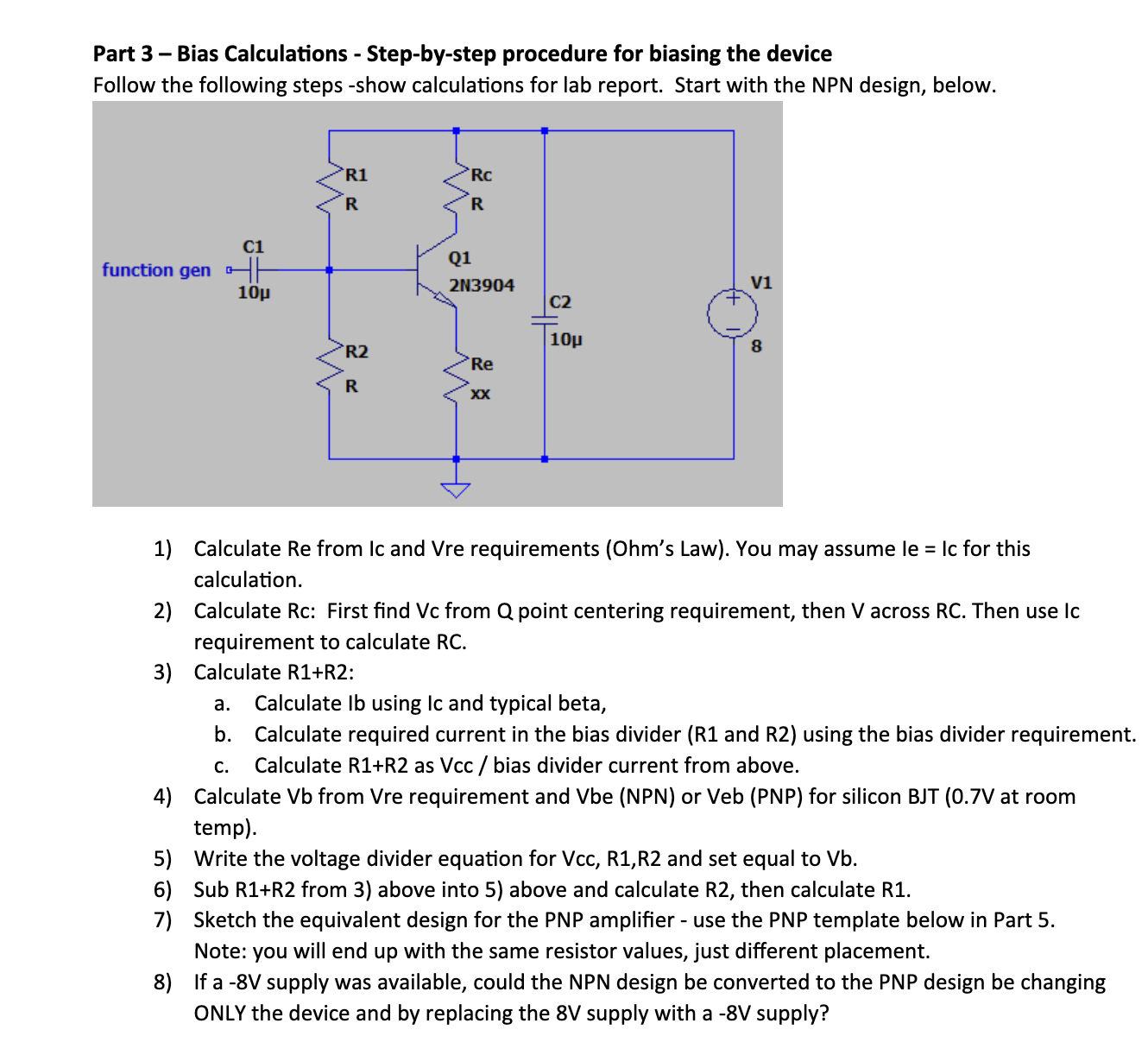
Follow the following steps show calculations for lab report. Start with the NPN design, below.
Calculate Re from Ic and Vre requirements Ohms Law You may assume le Ic for this
calculation.
Calculate Rc: First find Vc from Q point centering requirement, then V across RC Then use Ic
requirement to calculate RC
Calculate RR:
a Calculate Ib using Ic and typical beta,
b Calculate required current in the bias divider R and R using the bias divider requirement.
c Calculate RR as Vcc bias divider current from above.
Calculate Vb from Vre requirement and Vbe NPN or Veb PNP for silicon BJT V at room
temp
Write the voltage divider equation for VccRR and set equal to Vb
Sub RR from above into above and calculate R then calculate R
Sketch the equivalent design for the PNP amplifier use the PNP template below in Part
Note: you will end up with the same resistor values, just different placement.
If a V supply was available, could the NPN design be converted to the PNP design be changing
ONLY the device and by replacing the V supply with a V supply?
Step by Step Solution
There are 3 Steps involved in it
1 Expert Approved Answer
Step: 1 Unlock

Question Has Been Solved by an Expert!
Get step-by-step solutions from verified subject matter experts
Step: 2 Unlock
Step: 3 Unlock