

Question: Please answer all parts ( show all work ) and do not use any responses / solutons available on the site as they are incorrect.
Please answer all parts show all work and do not use any responsessolutons available on the site as they are incorrect. Use all attached images for extra info.
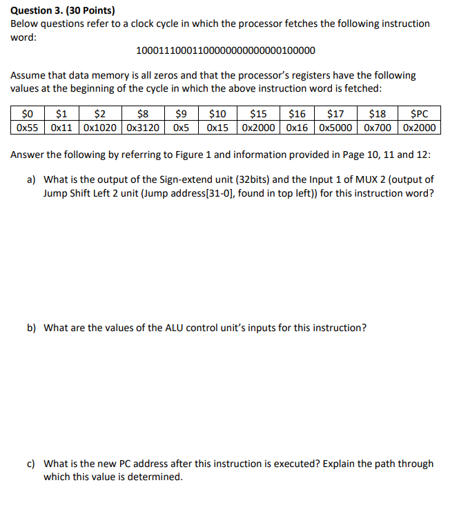
Below questions refer to a clock cycle in which the processor fetches the following instruction
word:
Assume that data memory is all zeros and that the processors registers have the following
values at the beginning of the cycle in which the above instruction word is fetched:
a What is the output of the Signextend unit bits and the Input of MUX output of
Jump Shift Left unit Jump address found in top left for this instruction word?
b What are the values of the ALU control units inputs for this instruction?
c What is the new PC address after this instruction is executed? Explain the path through
which this value is determined.
d For each MUX MUX to MUX show the values of its data output during the
execution of this instruction and these register values.
e For the ALU and the two add units, what are their data input values?
f What are the values of all inputs both data and control signals for the Registers unit? Question Points
Below questions refer to a clock cycle in which the processor fetches the following instruction
word:
Assume that data memory is all zeros and that the processor's registers have the following
values at the beginning of the cycle in which the above instruction word is fetched:
Answer the following by referring to Figure and information provided in Page and :
a What is the output of the Signextend unit bits and the Input of MUX output of
Jump Shift Left unit Jump address found in top left for this instruction word?
b What are the values of the ALU control unit's inputs for this instruction?
c What is the new PC address after this instruction is executed? Explain the path through
which this value is determined. d For each MUX MUX to MUX show the values of its data output during the
execution of this instruction and these register values.
e For the ALU and the two add units, what are their data input values?
f What are the values of all inputs both data and control signals for the "Registers" unit? Figure Single Cycle Implementation of MIPS Processor
Table ALU and ALUop Control SignalstableOp:TLB rs:mfccfcmtcctc
tableop:Rformat funct:tabletableshift leftlogicaltableshift rightlogicalsra,sllvsrlvsravtablejumpregisterjalr,,,syscall,break,,mfhi,mthi,mflo,mtlo,,,,mult,multu,div,divu,,,,add,addu,subtract,subu,and,orxor,not or norset lttableset I. tunsigned
Table MIPS Instruction Encoding
Step by Step Solution
There are 3 Steps involved in it
1 Expert Approved Answer
Step: 1 Unlock

Question Has Been Solved by an Expert!
Get step-by-step solutions from verified subject matter experts
Step: 2 Unlock
Step: 3 Unlock